


 Mean Stack Development
 Vue JS Development
 Javascript Development
 React JS Development
 Angular JS Development
 Next JS development
 Java Development
 Python Development
 Django Development
 Cherrypy Development
 C# Development
 ASP.NET Development
 NodeJS Development
 Laravel Development
 CodeIgniter Development
 Zend Development
 Ruby on Rails Development
 CakePHP Development
 PHP Website Development
 Symfony Development
 Drupal Development
 Joomla Development
 Wordpress Development
 .NET Nuke Development
 Kentico
 Umbraco
 .NET MAUI Development
 Xamarin Application Development
 iOS Application Development
 Android Application Development
 Android Wear App Development
 Ionic Development
 iBeacon Application Development
 Universal Windows Platform (UWP)
 Kotlin Application Development
 Swift Application Development
 Flutter Application Development
 PWA Application Development
 Flutter Health Tech & Wearable App Development Company
 React Native Health Tech Wearable App Development
 Offshore Software Development
 Custom Application Development
 Front-End Development
 Full Stack Development
 AI & Machine Learning
 Custom CRM Solutions
 Flask Software Development
 Electron JS Development
 ChatGPT Development
 Telemedicine App Development
 Build Smart Telemedicine Platform
 Beauty & Salon App Solutions
 Hire Workato Experts
 Magento Development
 Magento 2.0 Development
 Magento Enterprise
 Shopping Cart Development
 Prestashop Development
 Shopify Development
 Open Cart Development
 WooCommerce Development
 BigCommerce Development
 NopCommerce Development
 Virto Commerce Development
 AspDotNetStorefront Development
 .NET Application Development
 Microsoft Dynamics CRM
 VB .NET Development
 Sharepoint Migration
 ASP.NET Core Development
 ASP.NET MVC Development
 AJAX Development
 Agile Development
 Microsoft Bot
 Microsoft Blazor
 Microsoft Azure Cognitive
 HTML 5
 UI/UX Design
 Graphic Design
 Adobe Photoshop
 XML Application Development
 Cloud Computing Solutions
 Azure Cloud App Development
 AWS Development
 Google Cloud Development
 Certified AWS IoT Services Developers
 DevOps Consulting & Development
 Kubernetes Consulting & Services
 SQL Programming Development
 MySQL Development
 MongoDB Development
 Big Data
 Robotic Process Automation
 Social Media Marketing
 Search Engine Optimization
 QA Testing
 Software Testing
 Software Security
 Maintenance And Support
 I.T. Consulting Services
 Business Intelligence
 YII Development
 Data Analysis
 Alexa Skills Development
 On Demand App for Mobile repairing services
 On Demand App for Car Service Booking
 On Demand App for Cleaning Services
 On Demand App for Pharmacy
 On Demand Dedicated Developers
 On Demand Lawyer App Development












 Nuki Smart Lock
 Salto Smart Lock
 TTlock Smart Lock
 NFC App Development
 Custom IOT Enabled Smart Lock
 Smart Locker Solutions
 Hospital Smart Lock Systems
 Hotel Smart Lock Systems
 Smart Home & Office Locks
 Smart Access for Schools & Colleges
 Unloc Smart Lock Integration
 Yale & August Smart Lock Integration
 Populife Smart Lock Integration
 Smart Lock Hardware Development
 Dairy IoT Solutions
 Agri IoT & AI Solutions
 Weather & Climate Solutions
 Water & Waste Management Solutions
 RaspBerry Pi
 Firmware Software Development
 ESP 32 Software Development
 Embedded Development
 Internet of Things
 Smart IoT Development
 IoT Sensor Integration & Development Solutions
 Smart IoT System Development for HVAC
 Tuya IoT App Development
 Particle IoT SDK
 IoT Development with AI
 Smart Pet GPS Tracker
 Dairy GPS Tracking Solutions
 GPS Fleet Management Software
 Car Rental & Subscription Solutions
 Car Buy & Sell Marketplace Development
 AI-Powered Car Wash App Development
 PCB Design & Fabrication
 IoT AC Automation
 AI–IoT Painting Solutions
 IoT Wearable Hardware & App Development
 HVAC Automation & AI Control Systems
 Smart Home IoT Engineering
 AI Embedded Systems
 AI Hardware Design Service
 Advanced IoT Hardware & Firmware Development
 Device Driver Development Services
 NXP i.MX RT Firmware & Hardware Services
 Microchip PIC & AVR Development
 Hire IoT Architects
 IoT Cloud & Infrastructure Solutions
 Infineon XMC / AURIX Development Services
 Matter & Thread IoT Services
 Native IoT Mobile App Development (BLE & Wi-Fi)
 Snapdragon IoT Firmware Development
 Renesas RA/RX Firmware Services
 Silicon Labs EFR32 Development Services
 Smart Wearable App Development
 Smart IoT Meters
 Smart Healthcare Wearable App Development
 Health Care Monitoring System
 Fitness Tracking App Development
 Smart Home Automation Apps
 nRF PCB Design
 ESP32 PCB Design
 Embedded Wearables Engineers
 Rental Property Management System
 Building Management System
 Smart Lighting Development
 Infineon Semiconductor Firmware Development Services
 Custom Camera Development: Hardware, Firmware & PCB Prototyping
 Smart Security Camera SDK
 Nordic Semiconductor SDK
 Infineon SDK
 Arduino SDK
 NFC Lock Integration
 Kerong Lock Integration
 IoT & AI Solutions for Manufacturing
 Smart Inventory & Logistics Solution
 Food & Beverage Industry Solutions
 Smart Hospitality Solutions
 Smart Property Management
 Custom Smart Home IOT SDK
 Smart IoT & AI in Healthcare
 AI-Powered Security Solutions
 Smart Home Safety & AI
 Veterinary Clinic Management (AI)
 Pet Care System (AI & IoT)
 Pet Training & Adoption (AI)
 Healthcare IoT Development
 Event Management Software
 Money Remittance App
 Money Lending App Development
 Utility and Bill Payment App
 IoT Mobile App Development (Flutter & React Native)
 AI & IoT Retail Solutions
 Smart EV App Development
 Smart Solar IoT & AI Solutions
 IoT-Based Energy Systems
 Smart Energy & Utilities Solutions
 6G Solutions
 IoT Security Solutions
 AI-Powered Lottery App Development
 AI-Sports Fitness Club Management
 Travel
 Real Estate
 Medical & Healthcare
 e-Learning
 Consumer Products
 Finance
 Automobile
 Media & Entertainment
 Billing Software
 Enterprise Resource Planning (ERP)
 Augumented & Virtual Reality
 Point of Sale(POS) Development
 Learning Management System
 EV Charging Solutions
 About Us
 Partners & Certifications
 Quality Assurance
 Our Clients & Testimonials
 Development Process
 Our Products
 Social Responsibility
 Work Ethics
 Vision & Mission
 Awards
 Live Project Demos
 Contact Us
 Case Studies
 Portfolio
 Blog
PCB Design Review, EMI/EMC & Signal Integrity Analysis Services
A PCB can also comply with its requirements and still not work in practice, either in testing, certification or installation. Design-rule software indicates that the design follows the prescribed rules.
But this does not guarantee that an antenna will work in an enclosure, or that a switching regulator will be quiet when loaded down, or that a differential interface has adequate margins or that every production batch can be qualified the same way.
Adequate Infosoft provides PCB design review, EMI/EMC investigation, signal integrity analysis and production-readiness assessment for startups, OEMs and engineering teams.
We review new layouts before fabrication, investigate failed prototypes and help improve existing boards before certification or volume production.
Our engineers work with wireless IoT devices, medical wearables, industrial controllers, cameras, robotics, motor-control systems and connected consumer products. Every review is built around the product's interfaces, operating environment, enclosure and production plan.
Let's Work Together!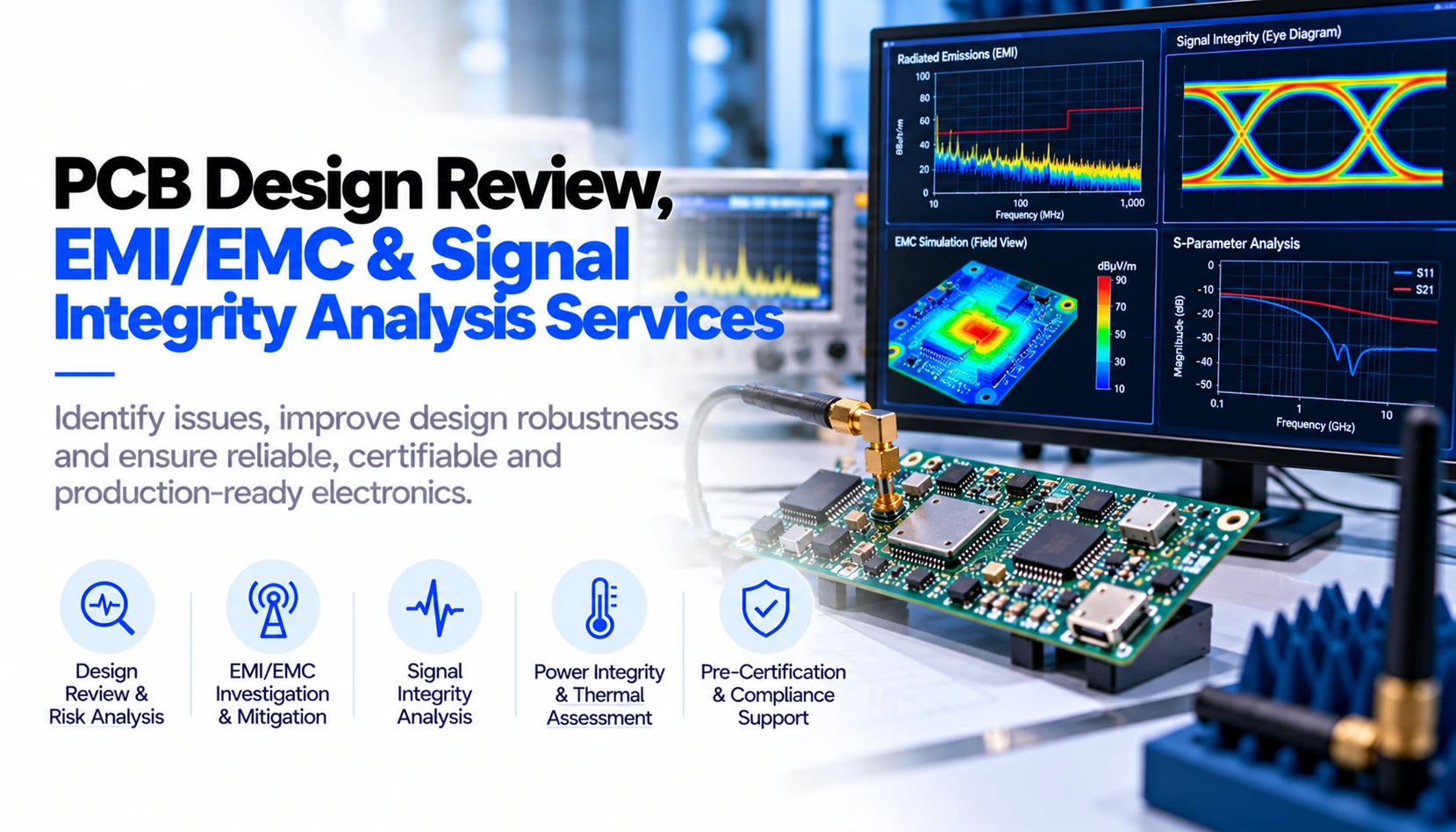
What is the Scope of a Professional PCB Design Review?
A well conducted review will look at more than just the visuals, it will relate the schematic and layout to the mechanical design and behavior of firmware, and manufacturing.
The aspects that can be reviewed include:
Schematic correctness and parts parameters Placement and layout of PCB Connections with controlled impedance Signal and power integrity Integration and tuning of RF antennas EMI emissions and immunity problems Thermal behavior PCB stack-up and reference planes Component lifecycle and availability DFM and DFT Accessibility of test points Programming and provisioning Potential production yield problems The documentation of design and right to it
The findings are grouped according to their severity and followed by practical advice. If some conclusions cannot be drawn from the documents, we specify the measurement that will prove or disprove our hypothesis.
Controlled-Impedance and Signal Integrity Review
Just like the way in which electrical signals travel through wires is influenced by the electrical characteristics of the circuit, high-speed signals behavior doesn't solely depend on wires either. Traces, pins, connectors, and reference planes create the electrical channel.
This review covers interface-specific requirements for USB, Ethernet, MIPI, DDR, LVDS, CAN, and some other digital connections.
Our work validates so-called impedance targets, geometry of differential pairs, length limitations, reference plane continuity, via transition process, distances between the signals, termination process, and connector placement.
Length matching is not the only principle taken into account; while using pairs correctly matched in length, it is necessary to avoid different plane splitting, significant via stubs, and incorrect stack-up.
In situations when modeling can be performed and it is possible to acquire the needed models, signal integrity analysis can be conducted.
The document must include the assumptions made in the process of creating a model and all components employed for the analysis.
Power Integrity and Thermal Review
Many apparent signal failures begin with the power-delivery network.
We review regulator selection, power sequencing, current paths, decoupling, bulk capacitance, plane connections and switching-loop geometry. Particular attention is given to processors, radios, motors, cameras and LED drivers that create changing current demand.
Thermal analysis considers component losses, copper spreading, thermal vias, airflow and enclosure contact. A device tested on an open bench may run considerably hotter once installed in a sealed housing.
Power and thermal findings are therefore evaluated under realistic operating modes, including wireless transmission, charging, processing peaks and fault conditions.
RF Antenna Placement and Matching Review
Wireless performance involves more than just choosing a certified module or copying a reference antenna.
The review covers the antenna location, keep-out zones, the layout of the ground plane, routing of the feed, matching circuits, nearby batteries, connectors, interconnecting cables, and enclosure materials.
We also address whether the final product could be tested and adjusted. For custom RF paths, controlled routing, and matching should be designed according to the actual PCB stack-up. Antenna performance should be verified in the final enclosure because plastic, metal, people, and position could alter its properties.
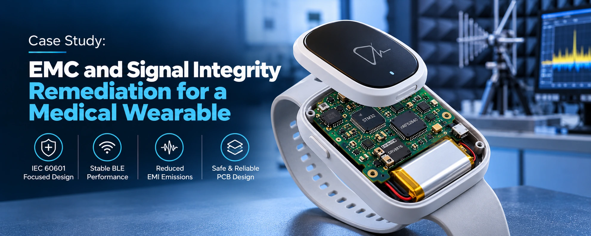
Case Study: EMC and Signal Integrity Remediation for a Medical Wearable
Client Situation and Initial Review
Adequate Infosoft was asked to review an existing BLE-enabled medical wearable developed by a confidential healthcare-device company.
The medical device contained an STM32L496 chip, Nordic nRF52840 chip, DRV8876 stimulator, rechargeable 500mAh battery and auxiliary power management circuits. Although the circuit board was already designed, it had to comply with IEC 60601 certification requirements for safety and EMC.
The assessment showed that patient-connected circuits, wireless systems, and USB power connections were not isolated properly. There were problems with emitted radiation levels from the circuit board as well as issues with Bluetooth communication during stimulation.
EMI Measurements and Root-Cause Analysis
The first open-board pre-compliance scan identified three important emissions:
52.1 dBµV/m at 480 MHz against a 46 dBµV/m limit 49.3 dBµV/m at 2.45 GHz against a 47 dBµV/m limit 44.2 dBµV/m at 122 MHz against a 43 dBµV/m limit
The 480 MHz emission was traced to harmonics associated with the TPS63900 switching converter and insufficient input filtering.
At 2.45 GHz, the review identified antenna-network and ground-stitching concerns around the nRF52840 radio. The 122 MHz problem involved clock-related energy escaping through the unshielded programming connection.
A separate coexistence problem occurred during stimulation. The H-bridge switching activity introduced ground disturbance into the shared digital domain. BLE packet-error rate increased from approximately 0.1% to 15%, producing connection drops.
PCB and Circuit Remediation
The redesign featured an introduction of a ferrite bead and capacitors at power inlet, a new arrangement of nRF52840 matching network, and also the addition of some filtering close to SWD programming header.
High-frequency wiring was placed at more appropriately referenced internal zones of the six-layer stack-up design. The ground was split into logic and patient side domains and an external 32 kHz crystal was introduced to strengthen radio timing precision.
The safety redesign added digital isolation and an isolated DC-DC supply. A routed PCB slot and revised copper clearance increased the relevant creepage distance from 2.1 mm to 10.2 mm.
Battery safety was also addressed by reducing charge current, adding temperature monitoring and incorporating independent over-temperature protection.
Verified Outcome and Production Preparation
During the second enclosed pre-compliance scan, the measured emissions fell to:
38.2 dBµV/m at 480 MHz, providing a 7.8 dB passing margin 42.1 dBµV/m at 2.45 GHz, providing a 4.9 dB margin 39.5 dBµV/m at 122 MHz, providing a 3.5 dB margin
In the worst-case scenario, the BLE packet error rate was lowered to 0.2%, and the published case study shows no disconnects during the 72-hour soak test.
The engagement also included the generation of specifications for dielectric strength, leakage current and continuity measurements, as well as guidance on the fixture for the contract manufacturer.
The project is a clear indication of what a proper PCB review should be able to achieve; find possible failure modes, change the circuit design and validate the results by means of repeatable testing.
Case Study URL: iec-60601-wearable-remediation-nrf52840-stm32
Relevant Case Studies That Demonstrate Our Review Experience
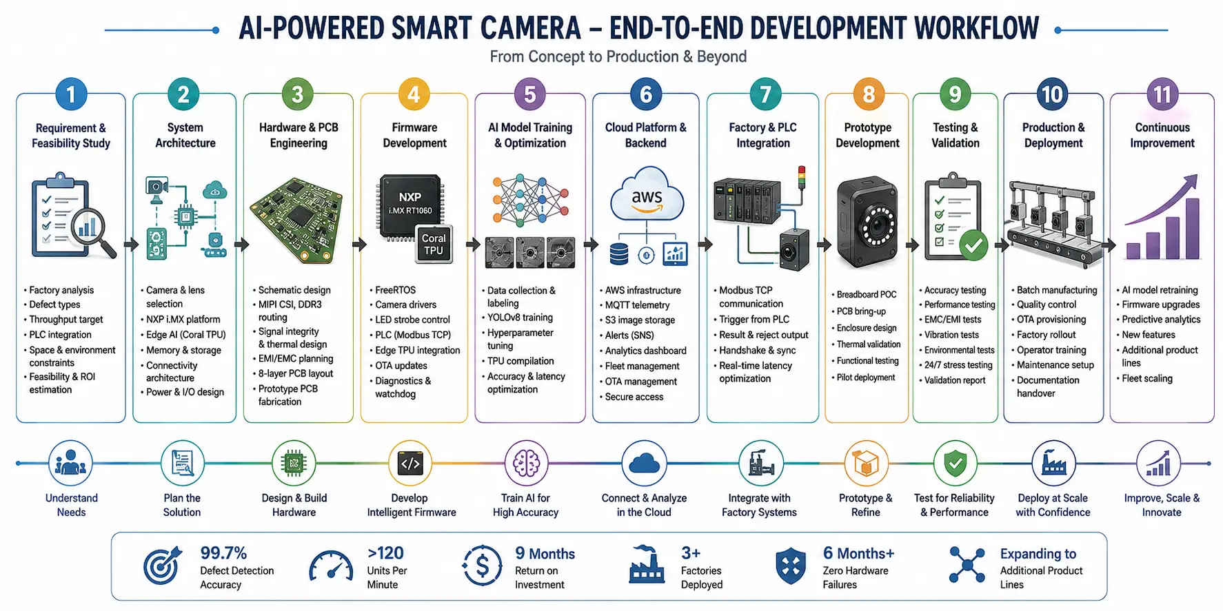
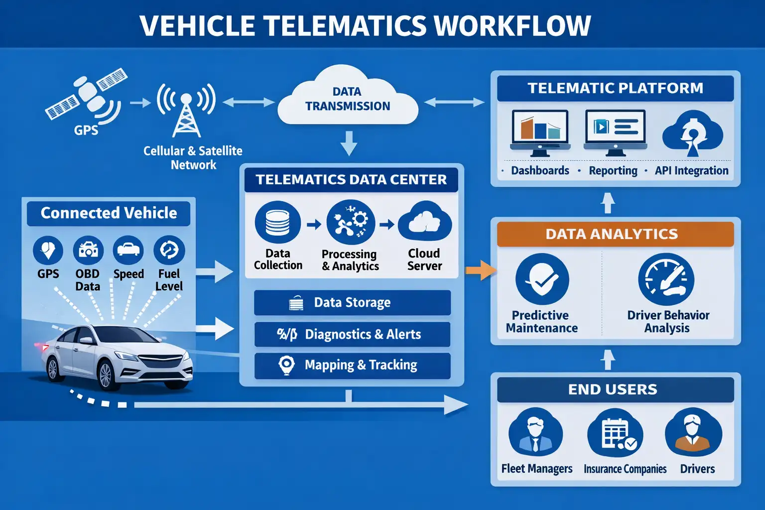
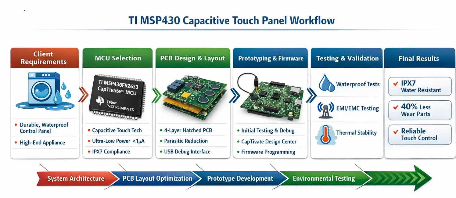
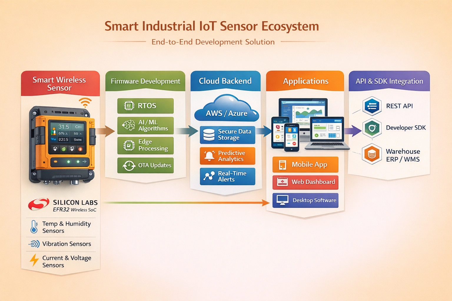
The following published projects demonstrate practical experience with signal integrity, EMC, grounding, thermal analysis and board validation.
Manufacturing Review: Where Good Layouts Become Good Products
The thought process of professional PCB customers includes the assessment of production and testing capabilities that PCB manufacturers possess rather than just determining the ability of one prototype to perform.
Availability of Components
We analyze the lifecycle status of components involved as well as the lead times, authority of suppliers, and dependence on alternatives. Potential features of alternatives are identified to confirm that electrical, mechanical, thermal, and firmware compatibility is ensured.
DFM and DFT
The Design for Manufacturing process considers manufacturing and assembly limitations like sizes of holes, clearances for solder mask, placement of components, panelisation, and access for inspection.
While the Design for Test process highlights power measurements, programming, calibration faults, and functional verification.
Test-Point Accessibility
Test points must be placed by the fixture that will reach them without interrupting any signals critical to the functioning of the device. Great caution has to be exercised in case of high-speed interfaces since adding unnecessary pads and stubs may have a negative effect on the channel.
Factory Programming
We review access to SWD, JTAG, UART or other programming interfaces, along with boot configuration, firmware verification, unique device identities and credential provisioning.
Production Yield
Pilot-build results should record solder defects, programming failures, rework and functional-test outcomes. Yield decisions should be based on production data rather than a single successful engineering sample.
Complete Title of Design Files
The ownership and transfer of design files should be defined before the start of the project. Deliverables can consist of editable schematics, original PCB documents, libraries, stacking information, production outputs and BOM basis, manuals for assembly, testing and updates.
Tools of other companies, licenses for use of libraries and manufacturer's information should also be clearly indicated.
Deliverables Offered in the PCB Assessment
The contents of a review package depend on the nature of the project:
Inspected schematic and PCB layout documents Risk severity rankings Recommendations regarding stack-up and impedance Methods to improve electromagnetic interference and compatibility Advice on signal and power integrity Comments on RF and antennas Tips on heat removal and component placement Recommendations regarding design for manufacturing and design for testing Recommended tests and measurement conditions Implementation assistance and recommendations regarding priority of modifications
Request an Independent PCB Review
Before proceeding with the building, certification and production, you should let Adequate Infosoft identify design risks that cannot be detected by means of automated rule checks.
Send us your schematic, PCB files, stack-up, BOM, enclosure data and any test results available. We are able to provide a review of your product which covers all aspects of electrical performance, as well as compliance-related issues, manufacturability, testing, and ownership issues.
Frequently Asked Questions
Both processes have their importance. The review of schematics and architecture identifies critical problems long before the routing takes place. The review after the layout phase assesses the quality of the file in terms of routing, return paths, thermal properties, and its readiness for fabrication.
No responsible engineering company should guarantee a test result without evidence. We reduce risk through design review, simulation where appropriate, prototype measurement and pre-compliance testing.
Absolutely! The independent review can be carried out without having to replace the initial designer. Recommendations can be provided upon completion of the review or implemented as part of the controlled changes.
Editorial Sources