


 Mean Stack Development
 Vue JS Development
 Javascript Development
 React JS Development
 Angular JS Development
 Next JS development
 Java Development
 Python Development
 Django Development
 Cherrypy Development
 C# Development
 ASP.NET Development
 NodeJS Development
 Laravel Development
 CodeIgniter Development
 Zend Development
 Ruby on Rails Development
 CakePHP Development
 PHP Website Development
 Symfony Development
 Drupal Development
 Joomla Development
 Wordpress Development
 .NET Nuke Development
 Kentico
 Umbraco
 .NET MAUI Development
 Xamarin Application Development
 iOS Application Development
 Android Application Development
 Android Wear App Development
 Ionic Development
 iBeacon Application Development
 Universal Windows Platform (UWP)
 Kotlin Application Development
 Swift Application Development
 Flutter Application Development
 PWA Application Development
 Flutter Health Tech & Wearable App Development Company
 React Native Health Tech Wearable App Development
 Offshore Software Development
 Custom Application Development
 Front-End Development
 Full Stack Development
 AI & Machine Learning
 Custom CRM Solutions
 Flask Software Development
 Electron JS Development
 ChatGPT Development
 Telemedicine App Development
 Build Smart Telemedicine Platform
 Beauty & Salon App Solutions
 Hire Workato Experts
 Magento Development
 Magento 2.0 Development
 Magento Enterprise
 Shopping Cart Development
 Prestashop Development
 Shopify Development
 Open Cart Development
 WooCommerce Development
 BigCommerce Development
 NopCommerce Development
 Virto Commerce Development
 AspDotNetStorefront Development
 .NET Application Development
 Microsoft Dynamics CRM
 VB .NET Development
 Sharepoint Migration
 ASP.NET Core Development
 ASP.NET MVC Development
 AJAX Development
 Agile Development
 Microsoft Bot
 Microsoft Blazor
 Microsoft Azure Cognitive
 HTML 5
 UI/UX Design
 Graphic Design
 Adobe Photoshop
 XML Application Development
 Cloud Computing Solutions
 Azure Cloud App Development
 AWS Development
 Google Cloud Development
 Certified AWS IoT Services Developers
 DevOps Consulting & Development
 Kubernetes Consulting & Services
 SQL Programming Development
 MySQL Development
 MongoDB Development
 Big Data
 Robotic Process Automation
 Social Media Marketing
 Search Engine Optimization
 QA Testing
 Software Testing
 Software Security
 Maintenance And Support
 I.T. Consulting Services
 Business Intelligence
 YII Development
 Data Analysis
 Alexa Skills Development
 On Demand App for Mobile repairing services
 On Demand App for Car Service Booking
 On Demand App for Cleaning Services
 On Demand App for Pharmacy
 On Demand Dedicated Developers
 On Demand Lawyer App Development












 Nuki Smart Lock
 Salto Smart Lock
 TTlock Smart Lock
 NFC App Development
 Custom IOT Enabled Smart Lock
 Smart Locker Solutions
 Hospital Smart Lock Systems
 Hotel Smart Lock Systems
 Smart Home & Office Locks
 Smart Access for Schools & Colleges
 Unloc Smart Lock Integration
 Yale & August Smart Lock Integration
 Populife Smart Lock Integration
 Smart Lock Hardware Development
 Dairy IoT Solutions
 Agri IoT & AI Solutions
 Weather & Climate Solutions
 Water & Waste Management Solutions
 RaspBerry Pi
 Firmware Software Development
 ESP 32 Software Development
 Embedded Development
 Internet of Things
 Smart IoT Development
 IoT Sensor Integration & Development Solutions
 Smart IoT System Development for HVAC
 Tuya IoT App Development
 Particle IoT SDK
 IoT Development with AI
 Smart Pet GPS Tracker
 Dairy GPS Tracking Solutions
 GPS Fleet Management Software
 Car Rental & Subscription Solutions
 Car Buy & Sell Marketplace Development
 AI-Powered Car Wash App Development
 PCB Design & Fabrication
 IoT AC Automation
 AI–IoT Painting Solutions
 IoT Wearable Hardware & App Development
 HVAC Automation & AI Control Systems
 Smart Home IoT Engineering
 AI Embedded Systems
 AI Hardware Design Service
 Advanced IoT Hardware & Firmware Development
 Device Driver Development Services
 NXP i.MX RT Firmware & Hardware Services
 Microchip PIC & AVR Development
 Hire IoT Architects
 IoT Cloud & Infrastructure Solutions
 Infineon XMC / AURIX Development Services
 Matter & Thread IoT Services
 Native IoT Mobile App Development (BLE & Wi-Fi)
 Snapdragon IoT Firmware Development
 Renesas RA/RX Firmware Services
 Silicon Labs EFR32 Development Services
 Smart Wearable App Development
 Smart IoT Meters
 Smart Healthcare Wearable App Development
 Health Care Monitoring System
 Fitness Tracking App Development
 Smart Home Automation Apps
 nRF PCB Design
 ESP32 PCB Design
 Embedded Wearables Engineers
 Rental Property Management System
 Building Management System
 Smart Lighting Development
 Infineon Semiconductor Firmware Development Services
 Custom Camera Development: Hardware, Firmware & PCB Prototyping
 Smart Security Camera SDK
 Nordic Semiconductor SDK
 Infineon SDK
 Arduino SDK
 NFC Lock Integration
 Kerong Lock Integration
 IoT & AI Solutions for Manufacturing
 Smart Inventory & Logistics Solution
 Food & Beverage Industry Solutions
 Smart Hospitality Solutions
 Smart Property Management
 Custom Smart Home IOT SDK
 Smart IoT & AI in Healthcare
 AI-Powered Security Solutions
 Smart Home Safety & AI
 Veterinary Clinic Management (AI)
 Pet Care System (AI & IoT)
 Pet Training & Adoption (AI)
 Healthcare IoT Development
 Event Management Software
 Money Remittance App
 Money Lending App Development
 Utility and Bill Payment App
 IoT Mobile App Development (Flutter & React Native)
 AI & IoT Retail Solutions
 Smart EV App Development
 Smart Solar IoT & AI Solutions
 IoT-Based Energy Systems
 Smart Energy & Utilities Solutions
 6G Solutions
 IoT Security Solutions
 AI-Powered Lottery App Development
 AI-Sports Fitness Club Management
 Travel
 Real Estate
 Medical & Healthcare
 e-Learning
 Consumer Products
 Finance
 Automobile
 Media & Entertainment
 Billing Software
 Enterprise Resource Planning (ERP)
 Augumented & Virtual Reality
 Point of Sale(POS) Development
 Learning Management System
 EV Charging Solutions
 About Us
 Partners & Certifications
 Quality Assurance
 Our Clients & Testimonials
 Development Process
 Our Products
 Social Responsibility
 Work Ethics
 Vision & Mission
 Awards
 Live Project Demos
 Contact Us
 Case Studies
 Portfolio
 Blog
Hire Custom PCB Design Engineers for Reliable, Manufacturable Electronics
A PCB can pass a design-rule check and still create expensive problems during assembly, testing or everyday use. An interrupted return path can increase emissions. A poorly positioned antenna can weaken wireless connectivity. An inaccessible programming interface can slow down every unit leaving the factory.
Adequate Infosoft provides custom PCB design engineering services for businesses developing connected devices, embedded systems, wearables and industrial electronics.
Our published portfolio contains hardware projects using ESP32, Nordic Semiconductor, and GPS tracking/sensor integration. The projects tie together PCB design with the firmware and software required to make it into a finished product.
In case you need an engineer who is well-versed in designing printed circuit boards to review your existing schematics or help design the circuit, it is essential to know your technical requirements and scope of work.
Critical review items will be verification of schematic design, component selection, board layout and routing, signal and power integrity, thermal management, manufacturability, and compliance with design standards.
Let's Work Together!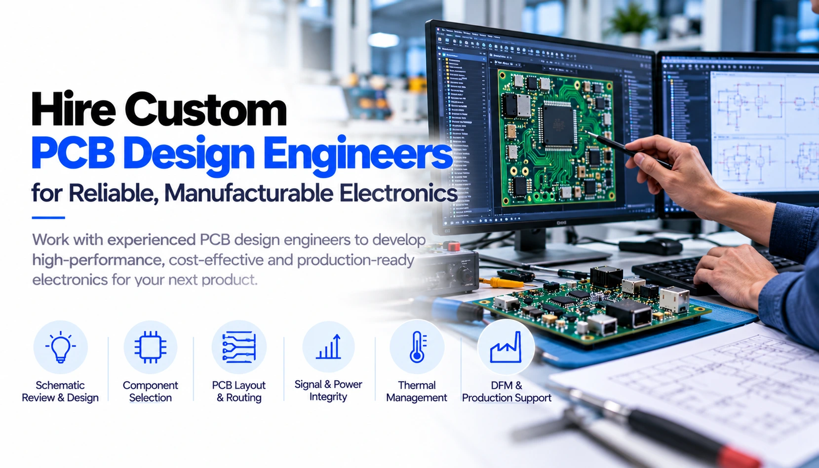
PCB Engineering Support Tailored to Your Needs
Different projects have different requirements for engineering services. An initial stage of conception might demand engineering decisions and components' evaluation. An already existing product might require changes to its layout, replacement of components or an independent review of its design.
The engagement of engineering in the process of PCB design might include:
Architecture and schematic design of electronics. Specification and development of a bill of materials. Multilayer board layout and routing. Placement of RF, mixed-signal and power circuits. Fabrication and assembly documentation. Bring-up and troubleshooting prototypes.
Before starting the work, it is important to specify who will be responsible for the circuit calculations, mechanical constraints, firmware interfaces and verification.
An Independent Engineer for PCB Design Review
Professional PCB Design Review Services
Would you like to hire an engineer to review your PCB designs? Our skilled hardware engineers will review your PCB layout, schematic, components, routing, and whether or not it is ready for manufacturing.
What We Review During Our PCB Design Review
Review of Schematic Design
Verify connections of circuitry, values of components, power allocation, and interfaces.
Review of PCB Layout Design
Analyze component placement, routing, grounding, and stack-up of layers.
Signal and Power Integrity
Analyze possible problems with high-speed signal, noise, and power integrity issues.
Design for Manufacturing (DFM)
Analyze clearances, drilling, footprints, and manufacturing aspects.
Thermal Management
Analyze heat-generating components.
Why Hire a PCB Design Review Engineer?
Independently conducted engineering review can identify design flaws, reduce the number of prototypes, and boost product reliability. We offer PCB designing services including Altium Designer, KiCad, Cadence Allegro, and OrCAD.
Our project-based or ongoing engineering review services can be tailored to meet your specific project requirements.
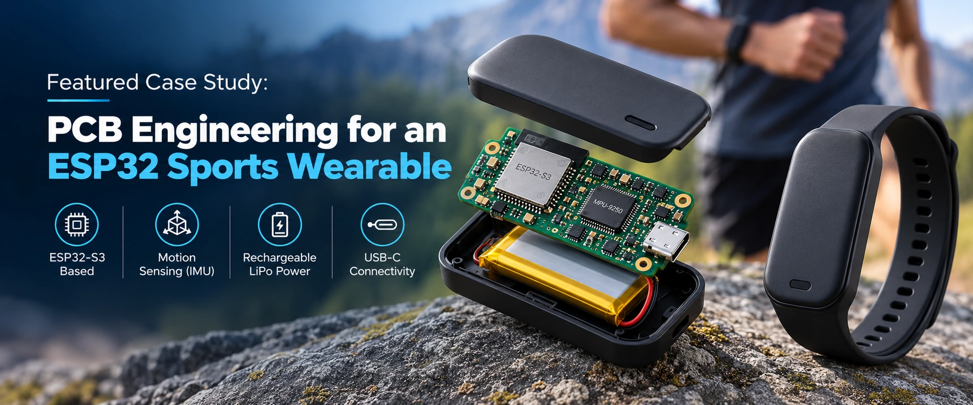
Featured Case Study: PCB Engineering for an ESP32 Sports Wearable
Client and Product Requirement
The client required a compact motion-sensing wearable for athletes and fitness users. Adequate Infosoft's published project describes an ESP32-based design combining an inertial measurement unit, rechargeable LiPo power and USB-C connectivity. The client retained responsibility for enclosure integration.
Published Engineering Scope
The device was implemented using an ESP32-S3-WROOM-1 and a MPU-9250 motion sensor. The power structure of this device included the use of a one-cell LiPo, USB-C charger, voltage regulation for the processing and sensing electronics.
The procurement of components was part of the assignment, together with compact mounting and consideration of the antenna needs of the wireless module. The publicized schedule spanned a period of four weeks.
Documented Handover
The listed deliverables included schematic files, PCB layout files, Gerber manufacturing data, a bill of materials with sourcing links and pick-and-place information.
This establishes a concrete design-and-documentation scope. The published delivery description should not be expanded into unreported claims about certified compliance, production yield or measured battery endurance.
Engineering Lessons for Similar Wearable Projects
The first thing one will have to do if he/she is purchasing and ordering the same item is the measurement process behavior that he/she will use.
The motion range, sampling rate, buffering and wireless data transfer affect the selection of sensors, processing and power consumption. All these things must be considered before signing the schematic.
Then the location becomes a trade-off between mechanical considerations, quality of measurements, possibility of charging and radio communications capability.
The motion sensor needs a right mechanical location relative to the object. The antenna needs some clearance. Neither of them can be regarded as something that one can consider at the very last minute.
The power budget should separate the continuous sensing mode, wireless activity, idle and charging modes. Battery life estimates start being really helpful once these operational modes are defined.
Acceptance Criteria for Your Own Engagement
Similarly, the statement of work must require that the design files be separated from the prototype assembly. This requires two deliverables with their own proofs.
As far as the design approval is concerned, consider the schematic review, layout review, footprints, and manufacturing package. Regarding the acceptance criteria of the prototype, consider establishing criteria for start-up, charging, sensor communications, programming, and wireless operation.
If the client provides the enclosure, consider defining the exchange process for mechanical issues such as the outline of the board, mounting, connectors, and component heights.
The bottom line here is to get PCB engineers working within an engineering scope. A thorough handover will make it easier for the next fabrication or revision, while acceptance criteria will make it easier to measure project completion.
Project reference: esp32-iot-sports-sensor-wearable
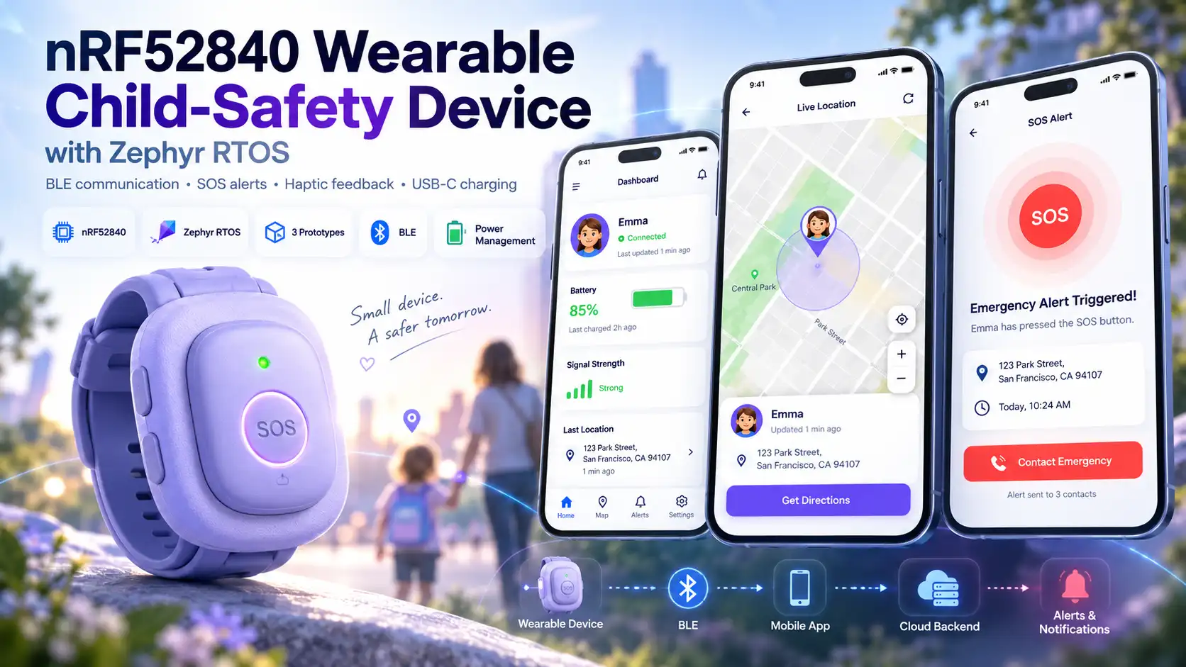
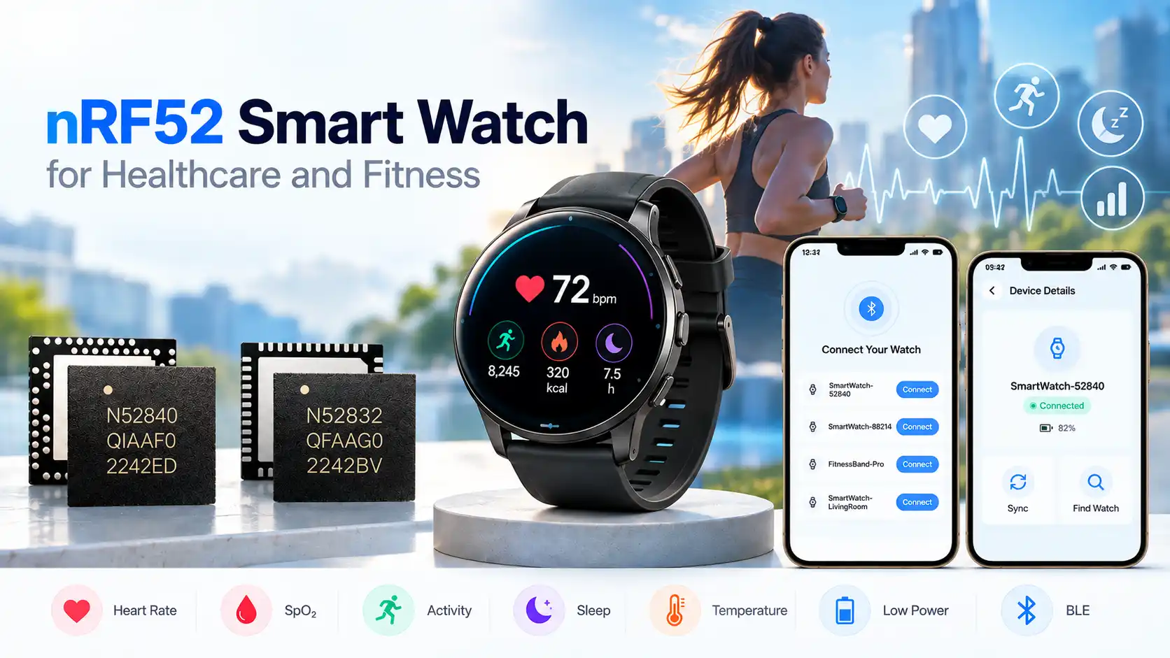
Relevant Projects Demonstrating Our Hardware Experience
Our published case studies provide examples of hardware engineering connected to wider product development. Each project has its own scope; use these references to assess experience relevant to your device.

Engineering the Details That Determine Board Performance
Controlled-Impedance Routing and PCB Stack-Up Planning
Controlled impedance starts with the proposed board construction. Dielectric thickness, copper thickness, material properties and reference-plane spacing affect the trace geometry required for a particular interface.
The designer should agree on a manufacturable stack-up with the fabricator before critical routing begins. Differential pairs also need suitable spacing, return paths and transition planning. Length matching alone does not establish signal integrity.
RF Antenna Placement and Matching
Wireless functionality also depends on the environment in which the antenna is used as well as on the antenna itself. Batteries, screens, metal housing and copper in the vicinity can affect antenna operation.
RF design needs to comply with reference guidelines for the selected component, leave space for antennas and include matching network footprints where needed. Test the assembled unit in its intended housing, a bare PCB does not reflect all operating conditions that the unit will face.
Signal Integrity, Power Integrity and EMI/EMC
High-speed signal edges and varying currents could cause any problems in what is otherwise a good design to become evident. Analyze continuity in the reference plane, placement of decoupling components, current loops through regulators, and connector interfaces.
In preparing for EMI/EMC issues, you have to consider the source, the path of coupling, and the affected circuits. Filters, protection, and shielding must have a specific objective. Compliance testing against the standards will be required eventually.
Thermal Management
Thermal design must take into account the modes of operation, environmental temperature, and enclosure constraints. Some regulators, chargers, processors, and power control switches may require copper spreading, thermal vias, or a mechanical path for heat transfer.
Only the ratings of the component temperatures cannot ensure that the board is reliable. Tests done on a prototype must validate the assumptions made during the design process.
Design for Assembly, Testing and Production Yield
Manufacturing issues are more difficult to address once the layout has been finalized. The design for manufacture (DFM) considerations should be taken into account right from the start – layout, spacing of components, solder mask clearance, and assembly access.
DFT should also be given equal consideration. Ensure that there are appropriate test points for critical power supplies, grounds, reset, programming, and diagnostics connections, sized and spaced appropriately for the suggested fixture.
There should also be some factory programming defined: the method of firmware upload, identification, configuration, and verification. If there are any security credentials involved, the provisioning requirements should be set in place before the production tooling is finalized.
Yield is a tangible result. Define criteria for pass and fail; define failure classifications and use the information from pilot build failures to identify recurring faults. Layout analysis facilitates this, but cannot guarantee any yield percentage.
Component Availability and Complete Design-File Ownership
Component choice must consider lifecycle position, distributor availability, packaging appropriateness, and alternatives. A substitute component is one that requires engineer approval since a matching description does not imply electrical or mechanical interchangeability.
Ownership of the file must also be as clear. Prior to engaging the PCB design company, ensure:
Editable native schematics and PCB designs. Customized symbols, footprints and libraries. BOM with manufacturer part numbers. Gerbers or other manufacturing files and drill files. Fabrication drawings, assembly drawings and placement files. Stack-up, impedance details and revision history. Test documents and firmware source code, if included.
IP ownership of the project and third party licensing issues should be specified in the contract. Manufacturing files are inadequate for simple modifications in the future design.
Discuss Your PCB Engineering Requirements
Share your current design and the problems you need to solve. Adequate Infosoft can discuss a PCB engineering scope covering design, prototyping and manufacturing preparation, with responsibilities and file handover defined before work begins.
Frequently Asked Questions
Yes. Start with the review of the schematic, footprint and requirements for identifying potential problems before starting routing.
The number of board interfaces, layers, mechanical limitations, documentation and validation effort are some factors influencing the cost estimation. Discuss revision cycles and acceptance criteria.
Not always. Proper engineering design eliminates unnecessary risk factors, whereas testing is performed to evaluate the final product along with enclosure, cables and modes of operation.
Provide your schematic or description of the product, board size, interfaces, power needs, quantities and target markets.