


 Mean Stack Development
 Vue JS Development
 Javascript Development
 React JS Development
 Angular JS Development
 Next JS development
 Java Development
 Python Development
 Django Development
 Cherrypy Development
 C# Development
 ASP.NET Development
 NodeJS Development
 Laravel Development
 CodeIgniter Development
 Zend Development
 Ruby on Rails Development
 CakePHP Development
 PHP Website Development
 Symfony Development
 Drupal Development
 Joomla Development
 Wordpress Development
 .NET Nuke Development
 Kentico
 Umbraco
 .NET MAUI Development
 Xamarin Application Development
 iOS Application Development
 Android Application Development
 Android Wear App Development
 Ionic Development
 iBeacon Application Development
 Universal Windows Platform (UWP)
 Kotlin Application Development
 Swift Application Development
 Flutter Application Development
 PWA Application Development
 Flutter Health Tech & Wearable App Development Company
 React Native Health Tech Wearable App Development
 Offshore Software Development
 Custom Application Development
 Front-End Development
 Full Stack Development
 AI & Machine Learning
 Custom CRM Solutions
 Flask Software Development
 Electron JS Development
 ChatGPT Development
 Veterinary Telemedicine App Development
 Build Smart Telemedicine Platform
 Beauty & Salon App Solutions
 Hire Workato Experts
 Magento Development
 Magento 2.0 Development
 Magento Enterprise
 Shopping Cart Development
 Prestashop Development
 Shopify Development
 Open Cart Development
 WooCommerce Development
 BigCommerce Development
 NopCommerce Development
 Virto Commerce Development
 AspDotNetStorefront Development
 .NET Application Development
 Microsoft Dynamics CRM
 VB .NET Development
 Sharepoint Migration
 ASP.NET Core Development
 ASP.NET MVC Development
 AJAX Development
 Agile Development
 Microsoft Bot
 Microsoft Blazor
 Microsoft Azure Cognitive
 HTML 5
 UI/UX Design
 Graphic Design
 Adobe Photoshop
 XML Application Development
 Cloud Computing Solutions
 Azure Cloud App Development
 AWS Development
 Google Cloud Development
 Certified AWS IoT Services Developers
 DevOps Consulting & Development
 Kubernetes Consulting & Services
 SQL Programming Development
 MySQL Development
 MongoDB Development
 Big Data
 Robotic Process Automation
 Social Media Marketing
 Search Engine Optimization
 QA Testing
 Software Testing
 Software Security
 Maintenance And Support
 I.T. Consulting Services
 Business Intelligence
 YII Development
 Data Analysis
 Alexa Skills Development
 On Demand App for Mobile repairing services
 On Demand App for Car Service Booking
 On Demand App for Cleaning Services
 On Demand App for Pharmacy
 On Demand Dedicated Developers
 On Demand Lawyer App Development


 Nuki Smart Lock
 Salto Smart Lock
 TTlock Smart Lock
 NFC App Development
 Custom IOT Enabled Smart Lock
 Smart Locker Solutions
 Hospital Smart Lock Systems
 Hotel Smart Lock Systems
 Smart Home & Office Locks
 Smart Access for Schools & Colleges
 Unloc Smart Lock Integration
 Yale & August Smart Lock Integration
 Populife Smart Lock Integration
 Smart Lock Hardware Development
 Dairy IoT Solutions
 Agri IoT & AI Solutions
 Weather & Climate Solutions
 Water & Waste Management Solutions
 RaspBerry Pi
 Firmware Software Development
 ESP 32 Software Development
 Embedded Development
 Internet of Things
 Smart IoT Development
 IoT Sensor Integration & Development Solutions
 Smart IoT System Development for HVAC
 Tuya IoT App Development
 Particle IoT SDK
 IoT Development with AI
 Smart Pet GPS Tracker
 Dairy GPS Tracking Solutions
 GPS Fleet Management Software
 Car Rental & Subscription Solutions
 Car Buy & Sell Marketplace Development
 AI-Powered Car Wash App Development
 PCB Design & Fabrication
 IoT AC Automation
 AI–IoT Painting Solutions
 IoT Wearable Hardware & App Development
 HVAC Automation & AI Control Systems
 Smart Home IoT Engineering
 AI Embedded Systems
 AI Hardware Design Service
 Advanced IoT Hardware & Firmware Development
 Device Driver Development Services
 NXP i.MX RT Firmware & Hardware Services
 Microchip PIC & AVR Development
 Hire IoT Architects
 IoT Cloud & Infrastructure Solutions
 Infineon XMC / AURIX Development Services
 Matter & Thread IoT Services
 Native IoT Mobile App Development (BLE & Wi-Fi)
 Snapdragon IoT Firmware Development
 Renesas RA/RX Firmware Services
 Silicon Labs EFR32 Development Services
 Smart Wearable App Development
 Smart IoT Meters
 Smart Healthcare Wearable App Development
 Health Care Monitoring System
 Fitness Tracking App Development
 Smart Home Automation Apps
 nRF PCB Design
 ESP32 PCB Design
 Embedded Wearables Engineers
 Rental Property Management System
 Building Management System
 Smart Lighting Development
 Infineon Semiconductor Firmware Development Services
 Custom Camera Development: Hardware, Firmware & PCB Prototyping
 Smart Security Camera SDK
 Nordic Semiconductor SDK
 Infineon SDK
 Arduino SDK
 NFC Lock Integration
 Kerong Lock Integration
 IoT & AI Solutions for Manufacturing
 Smart Inventory & Logistics Solution
 Food & Beverage Industry Solutions
 Smart Hospitality Solutions
 Smart Property Management
 Custom Smart Home IOT SDK
 Smart IoT & AI in Healthcare
 AI-Powered Security Solutions
 Smart Home Safety & AI
 Veterinary Clinic Management (AI)
 Pet Care System (AI & IoT)
 Pet Training & Adoption (AI)
 Healthcare IoT Development
 Event Management Software
 Money Remittance App
 Money Lending App Development
 Utility and Bill Payment App
 IoT Mobile App Development (Flutter & React Native)
 AI & IoT Retail Solutions
 Smart EV App Development
 Smart Solar IoT & AI Solutions
 IoT-Based Energy Systems
 Smart Energy & Utilities Solutions
 6G Solutions
 IoT Security Solutions
 AI-Powered Lottery App Development
 AI-Sports Fitness Club Management
 Travel
 Real Estate
 Medical & Healthcare
 e-Learning
 Consumer Products
 Finance
 Automobile
 Media & Entertainment
 Billing Software
 Enterprise Resource Planning (ERP)
 Augumented & Virtual Reality
 Point of Sale(POS) Development
 Learning Management System
 EV Charging Solutions
 About Us
 Partners & Certifications
 Quality Assurance
 Our Clients & Testimonials
 Development Process
 Our Products
 Social Responsibility
 Work Ethics
 Vision & Mission
 Awards
 Live Project Demos
 Contact Us
 Case Studies
 Portfolio
 Blog
Hire Embedded Wearables Engineers: Hardware, PCB & IoT Systems
Adequate Infosoft is a leading global technology partner where you can hire expert engineers focused on Embedded IoT Wearables. We help convert complex biometric and industrial needs into compact, high-performance wearable devices that meet or exceed your expectations.
With our expertise in multi-layer and rigid-flex PCB design, ultra-low-power circuit optimization and embedded firmware development we are able to help customers take their innovative idea and create a new electronic product that is ready for mass manufacture using one of the latest semiconductor platforms such as nRF52 Series SoC, ESP32 or STM32.
The foundation of our products is the quality of our hardware design, embedded engineering, and PCB engineering. If you need high-quality solutions in the wearable's area, you can hire our team of Embedded Wearable Engineers, who specialize in the design and development of all aspects of your IoT wearable's system.
As a full-service hardware and software development company, we offer everything necessary to build your solution in one place.
Let's Work Together!
Wearable PCB and Firmware Developers You Can Hire
The right team composition depends on what already exists. We can align developers around roles such as:
-
Hardware architect: Defines the MCU, radio, sensors, power tree and test strategy. -
PCB designer: Creates schematics, stack-up, layout and manufacturing documentation. -
RF/BLE engineer: Reviews antennas, matching, ground strategy, coexistence and RF results. -
Firmware developer: Builds drivers, RTOS tasks, BLE services, storage and diagnostics. -
Low-power engineer: Profiles current and optimizes wakeups, peripherals, radio and sensor schedules. -
Sensor engineer: Integrates PPG, ECG, temperature, IMU or pressure sensing and signal-quality logic. -
Validation engineer: Performs bring-up, fault isolation, current profiling and manufacturing-test development.
Roles may be combined or separated for precision analog, rigid-flex, multi-radio or regulated products.
Case Study: ESP32 Wearable Audio Prototype – Mixed-Signal PCB Design Showcase

ESP32 Wearable Audio Prototype
We recently partnered with a client developing an ESP32-based wearable audio prototype, focusing on delivering a compact, high-performance mixed-signal PCB design.
The client had desire to have their schematic and PCB designed with a professional electrical engineer with experience in working on cylindrical products that are approximately 10.5 mm high x 46 mm in diameter. Our team completed a complete design from concept to build to assist the customer in the development of a fully functional prototype of the produce.
Project Challenge
The wearable product consisted of a complete mixed signal audio chain that had an ADC and DAC to support a true mixed signal application.
A true mixed signal design is challenging because it must strategically combine different types of circuits (i.e. analog vs. digital) in a small cylindrical form factor and create a low noise environment while still operating within a highly noisy digital switching environment.
The products design included constraints from an ESP32 based microprocessor design, power management requirements, sensor integration, and enclosure design mechanical limitations therefore, the final design had to have the ability to be designed based on an initial prototype run to ensure reliability and acceptable signal integrity.
The Process We Followed
The first step was to review the client's high-level conceptual and technical requirements. We entered into a mutual non-disclosure agreement (NDA) with the client in order to protect any potentially sensitive information related to the product design, enabling us to then gain access to the complete system architecture, audio chain specifications, connectivity requirements, and constraints from all mechanical aspects.
The next step was to develop a complete schematic design by selecting components needed for the audio chain, (i.e., an appropriate set of low-noise ADC/DAC ICs) and designing appropriate passive filtering networks, including power supply filters decoupling and power supply conditioning were critical to the success of the audio chain.
Grounding schemes and routing of signals, as well as isolating the analog and digital domains to minimize inducement of noise or interference, were given careful consideration in the early stages of design.
After the schematic was approved, we transitioned into the PCB layout phase. As part of the PCB layout, we followed industry-standard best practices in mixed-signal design by ensuring:
The optimal layout of mixed-signal components (i.e., placing analog and digital components in such a way to minimize crosstalk). The routing of low-noise signals through the PCB. The creation of controlled impedance paths for high-speed digital signals. Adequate heating and electrical decoupling for reliable performance. Provision of test points and connectors to facilitate bench testing.
As we created the layout, we continually worked with the client and adjusted to the real-world limitations of the product and design iterations. Ultimately, both the electrical and mechanical aspects of the prototype product were achieved within the required small cylindrical package.
Outcome
The deliverables for the project included a complete set of schematics and PCB layout drawings for a low-noise mixed-signal audio chain, as well as documents related to the component selection and layout notes used to produce the prototype design.
The client was provided with a prototype-ready design that could be used for testing purposes in a smaller volume before moving onto larger production runs.
The work on this project highlights the experience we bring to designing wearable products using the ESP32 platform, as well as designing PCB layouts for mixed signals.
We were able to produce a feasible product under technical constraints through our extensive knowledge of low-noise mixed signal PCB layouts and the use of high-quality components. Finally, by utilizing proven signal integrity techniques and working collaboratively with our engineering partners, we were able to create a product ready for testing in a real environment.
Relevant Adequate Infosoft Case Studies
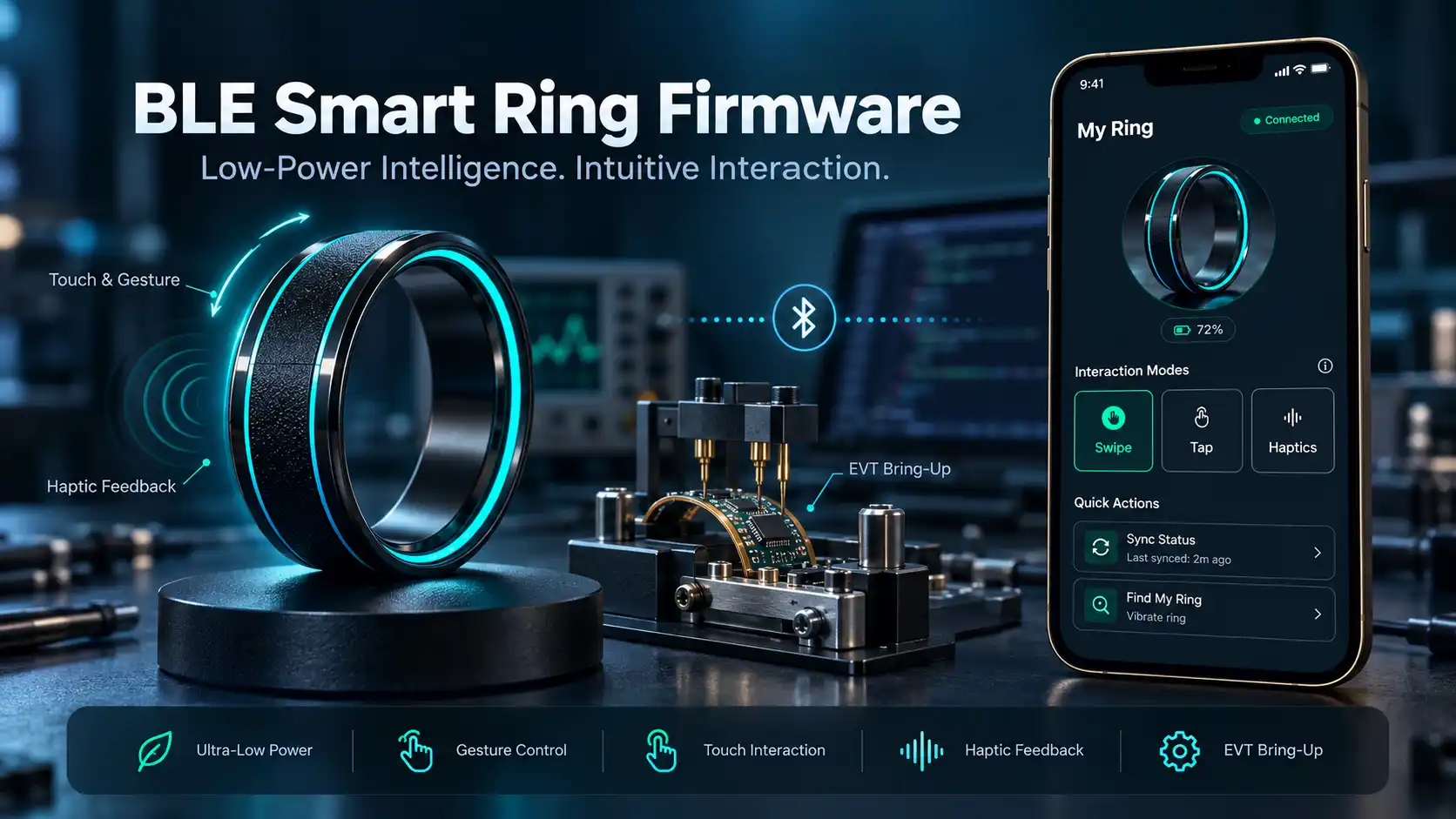
Nordic nRF52 BLE Smart Ring Firmware and EVT Support
Adequate Infosoft developed nRF52-class firmware for the BLE smart ring during the EVT process, as explained in the case study focused on the development of this wireless device.
The work included designing an architecture based on the event-driven principle and RTOS, implementing soft- and hardware control of LED, processing touch gestures, making the connection possible through BLE pairing and bonding, managing power consumption through peripheral power gating.
The team provided support with bringing up the board, mapping the pins, debugging the hardware and making necessary changes after the printed circuit board had been revised. Testing included power tests, tests of gesture performance and BLE stability, as well as tests related to long periods of inactivity.
Read Case Study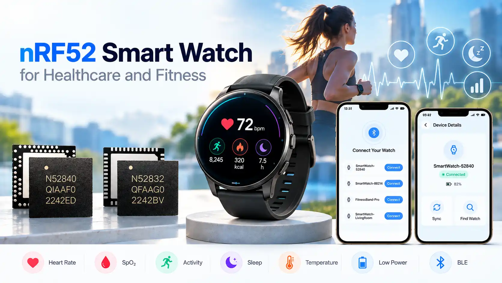
nRF52 Smartwatch Hardware and Firmware Development
The nRF52 smartwatch project was built using nRF52832/nRF52840 hardware, multilayer RF-enabled PCB design, a Bluetooth Low Energy antenna, IMU and heart rate sensors along with power management and charging capabilities.
The RTOS firmware implemented drivers for devices, BLE GATT functions for synchronization, active/idle/deep sleep modes, secure pairing and OTA handling. Sensor fusion was responsible for workout monitoring and jump analysis while prototypes and manufacturing documentation finalized the design for manufacturing.
This demonstrates coordination across hardware, embedded software, algorithms and handover.
Read Case Study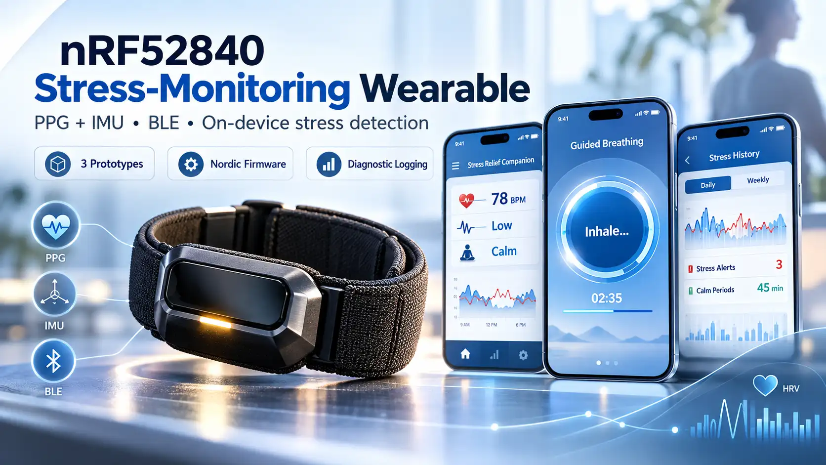
BLE Medical Wearable Design Remediation
The case study on medical wearables prepared by Adequate Infosoft covered the use of the nRF52840, STM32L496VG chipsets and a therapeutical stimulator powered by a battery. The engagement covered isolation, EMC, battery-management, BLE-coexistence and production-test issues resolved by means of a senior hardware review and risk mitigation.
This example is important for teams that have to use experienced design review but one project outcome is not enough to certify another product.
It is relevant evidence for teams that need experienced design-review support, although one project outcome does not guarantee certification for another product.
Read Case StudyWearable PCB Design Expertise
Miniaturized Schematic and Layout Design
We specialize in creating rigid, flexible, and rigid-flex circuit boards for applications like smart rings, smart bands, smart patches, smart tags, and 'smart clothing' modules. Our work involves using dense placement techniques and working with small pitch technology, controlled return strings, HDI technologies, bend-radiuses, and enclosure-aware test pads. The IPC provides separate guidelines for rigid, flexible, HDI, and RF boards, and customers have a chance to agree about any special requirements.
A board is analyzed as an assembly concerning the height of components, the surfaces facing the skin, the sealing, the charging contacts, flex zones, and accessibility. Early working with mechanical magazines reduces revisions that can affect the performance of antennas, sensors, or batteries.
RF, Antenna and Signal Integrity
It is important to note that human tissues, batteries, displays and metals can disrupt the operation of even the smallest antennas. Developers will need to consider locations for keep-outs, feed and matching networks, transmission lines, return paths and RF test access to ensure proper performance. The performance will only be validated in the given enclosure with the use of representative conditions.
For mixed-signal wearables, it is vital to separate sensitive analog channels from regulators, clocks, haptics and the paths radio currents. The area of concerns in this respect includes grounding, filtering, references and sampling timing.
Batteries, Charging, and Power Configuration
The power system may comprise Li-ion battery, charger, protections, fuel gauge, regulators, load switches and operational mode. The budgeting process is carried out based on operational states instead of relying on average current consumption; hence, thermal limits and peak signal or haptic current are considered.
Embedded Firmware Development for Wearables
Operating Systems, Talented Engineers and Device Operations
The firmware developers are utilizing Nordic nRF52/nRF53, STM32, ESP32 and other qualitative and appropriate formats by means of C/C++, vendor SDKs, Zephyr and other designs working on the principles of an OS.
The architecture guarantees that the separation is made for board support, drivers, services, application logic, connectivity, and diagnostics making the hardware revisions more manageable.
The scope can cover different drivers like I²C, SPI, UART, and ADC, peripherals like sensors, displays, and haptics, as well as others such as storage, touch and gestures, watchdogs, error recovery, manufacturing modes, and diagnostics.
The mobile, cloud, and testing divisions have the access to the interfaces.
BLE Connectivity and Secure OTA
We develop advertising, connections, GATT services, permissions, pairing, bonding, batching and reconnection. Payloads define byte order, timestamps, sequences, errors and versions. Secure OTA can include signed firmware, compatibility checks, resumable transfer, confirmation and rollback where hardware supports it.
Optimization of Low-Power Firmware
Battery life is calculated as a sum of time spent in advertising, transfer, sensing, processing, idle and sleeping. Current profiling uncovers unexpected wakeups, active peripherals, polling and too much radio activity.
Zephyr runtime power management can suspend inactive devices but requires correct implementations of drivers.
Optimization includes interrupts, FIFOs, sensor duty cycles, power domains, BLE parameters and batching. We report test conditions instead of claiming the runtime based on capacity calculations.
Embedded Wearables Solutions: Hardware, PCB & IoT Development – Contact Us
For your next wearable device development requirement, you can hire Embedded Wearables Engineers from us for trusted partner development.
As a full-stack software and hardware development company, we can provide all-in-one IoT wearable solution development. Our Engineers have all the required technical expertise in PCB design, hardware engineering, embedded firmware development and IoT integration to ensure that your wearable solution development will be done seamlessly from concept through the production of the product.
Our IoT Certifications Demonstrating Our Expertise
Our IoT certifications demonstrate our strong expertise in designing and developing reliable connected systems. They validate our skills in embedded hardware, wireless communication, and IoT architecture, ensuring we deliver secure, efficient, and production-ready solutions for modern smart devices and industrial IoT applications.
Frequently Asked Questions
Yes. We are able to address one gap in competencies or propose a full team. In systems design, however, multidisciplinary decision-making is preferred as PCB and firmware issues are interconnected.
Definitely. We are able to carry out an assessment of all documentation, replicate errors, and investigate technical debt. Having a hardware is a real advantage.
Definitely. Our work can cover the start of the product, revision management, tests and DFM coordination, test firmware, and issue resolution for mass manufacturing.
No responsible developer should guarantee these before measurement and formal testing. We define targets, engineer toward them and provide evidence under documented conditions. Accredited laboratories and authorized bodies determine certification results.
The ownership of intellectual property, third-party parts and handover conditions should be discussed and recorded in the contract. The deliverables list may explicitly cover editable design sources, firmware repositories and documentation of the build process.