














 Mean Stack Development
 Vue JS Development
 Javascript Development
 React JS Development
 Angular JS Development
 Next JS development
 Java Development
 Python Development
 Django Development
 Cherrypy Development
 C# Development
 ASP.NET Development
 NodeJS Development
 Laravel Development
 CodeIgniter Development
 Zend Development
 Ruby on Rails Development
 CakePHP Development
 PHP Website Development
 Symfony Development
 Drupal Development
 Joomla Development
 Wordpress Development
 .NET Nuke Development
 Kentico
 Umbraco
 .NET MAUI Development
 Xamarin Application Development
 iOS Application Development
 Android Application Development
 Android Wear App Development
 Ionic Development
 iBeacon Application Development
 Universal Windows Platform (UWP)
 Kotlin Application Development
 Swift Application Development
 Flutter Application Development
 PWA Application Development
 Flutter Health Tech & Wearable App Development Company
 React Native Health Tech Wearable App Development
 Offshore Software Development
 Custom Application Development
 Front-End Development
 Full Stack Development
 AI & Machine Learning
 Custom CRM Solutions
 Flask Software Development
 Electron JS Development
 ChatGPT Development
 Telemedicine App Development
 Build Smart Telemedicine Platform
 Beauty & Salon App Solutions
 Hire Workato Experts
 Magento Development
 Magento 2.0 Development
 Magento Enterprise
 Shopping Cart Development
 Prestashop Development
 Shopify Development
 Open Cart Development
 WooCommerce Development
 BigCommerce Development
 NopCommerce Development
 Virto Commerce Development
 AspDotNetStorefront Development
 .NET Application Development
 Microsoft Dynamics CRM
 VB .NET Development
 Sharepoint Migration
 ASP.NET Core Development
 ASP.NET MVC Development
 AJAX Development
 Agile Development
 Microsoft Bot
 Microsoft Blazor
 Microsoft Azure Cognitive
 HTML 5
 UI/UX Design
 Graphic Design
 Adobe Photoshop
 XML Application Development
 Cloud Computing Solutions
 Azure Cloud App Development
 AWS Development
 Google Cloud Development
 Certified AWS IoT Services Developers
 DevOps Consulting & Development
 Kubernetes Consulting & Services
 SQL Programming Development
 MySQL Development
 MongoDB Development
 Big Data
 Robotic Process Automation
 Social Media Marketing
 Search Engine Optimization
 QA Testing
 Software Testing
 Software Security
 Maintenance And Support
 I.T. Consulting Services
 Business Intelligence
 YII Development
 Data Analysis
 Alexa Skills Development
 On Demand App for Mobile repairing services
 On Demand App for Car Service Booking
 On Demand App for Cleaning Services
 On Demand App for Pharmacy
 On Demand Dedicated Developers
 On Demand Lawyer App Development











 Nuki Smart Lock
 Salto Smart Lock
 TTlock Smart Lock
 NFC App Development
 Custom IOT Enabled Smart Lock
 Smart Locker Solutions
 Hospital Smart Lock Systems
 Hotel Smart Lock Systems
 Smart Home & Office Locks
 Smart Access for Schools & Colleges
 Unloc Smart Lock Integration
 Yale & August Smart Lock Integration
 Populife Smart Lock Integration
 Smart Lock Hardware Development
 Dairy IoT Solutions
 Agri IoT & AI Solutions
 Weather & Climate Solutions
 Water & Waste Management Solutions
 RaspBerry Pi
 Firmware Software Development
 ESP 32 Software Development
 Embedded Development
 Internet of Things
 Smart IoT Development
 IoT Sensor Integration & Development Solutions
 Smart IoT System Development for HVAC
 Tuya IoT App Development
 Particle IoT SDK
 IoT Development with AI
 Smart Pet GPS Tracker
 Dairy GPS Tracking Solutions
 GPS Fleet Management Software
 Car Rental & Subscription Solutions
 Car Buy & Sell Marketplace Development
 AI-Powered Car Wash App Development
 PCB Design & Fabrication
 IoT AC Automation
 AI–IoT Painting Solutions
 IoT Wearable Hardware & App Development
 HVAC Automation & AI Control Systems
 Smart Home IoT Engineering
 AI Embedded Systems
 AI Hardware Design Service
 Advanced IoT Hardware & Firmware Development
 Device Driver Development Services
 NXP i.MX RT Firmware & Hardware Services
 Microchip PIC & AVR Development
 Hire IoT Architects
 IoT Cloud & Infrastructure Solutions
 Infineon XMC / AURIX Development Services
 Matter & Thread IoT Services
 Native IoT Mobile App Development (BLE & Wi-Fi)
 Snapdragon IoT Firmware Development
 Renesas RA/RX Firmware Services
 Silicon Labs EFR32 Development Services
 Smart Wearable App Development
 Smart IoT Meters
 Smart Healthcare Wearable App Development
 Health Care Monitoring System
 Fitness Tracking App Development
 Smart Home Automation Apps
 nRF PCB Design
 ESP32 PCB Design
 Embedded Wearables Engineers
 Rental Property Management System
 Building Management System
 Smart Lighting Development
 Infineon Semiconductor Firmware Development Services
 Custom Camera Development: Hardware, Firmware & PCB Prototyping
 Smart Security Camera SDK
 Nordic Semiconductor SDK
 Infineon SDK
 Arduino SDK
 NFC Lock Integration
 Kerong Lock Integration
 IoT & AI Solutions for Manufacturing
 Smart Inventory & Logistics Solution
 Food & Beverage Industry Solutions
 Smart Hospitality Solutions
 Smart Property Management
 Custom Smart Home IOT SDK
 Smart IoT & AI in Healthcare
 AI-Powered Security Solutions
 Smart Home Safety & AI
 Veterinary Clinic Management (AI)
 Pet Care System (AI & IoT)
 Pet Training & Adoption (AI)
 Healthcare IoT Development
 Event Management Software
 Money Remittance App
 Money Lending App Development
 Utility and Bill Payment App
 IoT Mobile App Development (Flutter & React Native)
 AI & IoT Retail Solutions
 Smart EV App Development
 Smart Solar IoT & AI Solutions
 IoT-Based Energy Systems
 Smart Energy & Utilities Solutions
 6G Solutions
 IoT Security Solutions
 AI-Powered Lottery App Development
 AI-Sports Fitness Club Management
 Travel
 Real Estate
 Medical & Healthcare
 e-Learning
 Consumer Products
 Finance
 Automobile
 Media & Entertainment
 Billing Software
 Enterprise Resource Planning (ERP)
 Augumented & Virtual Reality
 Point of Sale(POS) Development
 Learning Management System
 EV Charging Solutions
 About Us
 Partners & Certifications
 Quality Assurance
 Our Clients & Testimonials
 Development Process
 Our Products
 Social Responsibility
 Work Ethics
 Vision & Mission
 Awards
 Live Project Demos
 Contact Us
 Case Studies
 Portfolio
 Blog
Blog
IoT Wearable PCB Designing & Prototyping Services
Adequate Infosoft is a globally trusted IoT wearable PCB design and prototyping company. We engineer compact, production-ready printed circuit boards for wearable devices, from fitness trackers and smartwatches to medical-grade health monitors and industrial wearables.
Our hardware engineering team takes your product idea from initial schematic all the way through to a verified, mass-production-ready PCBA.
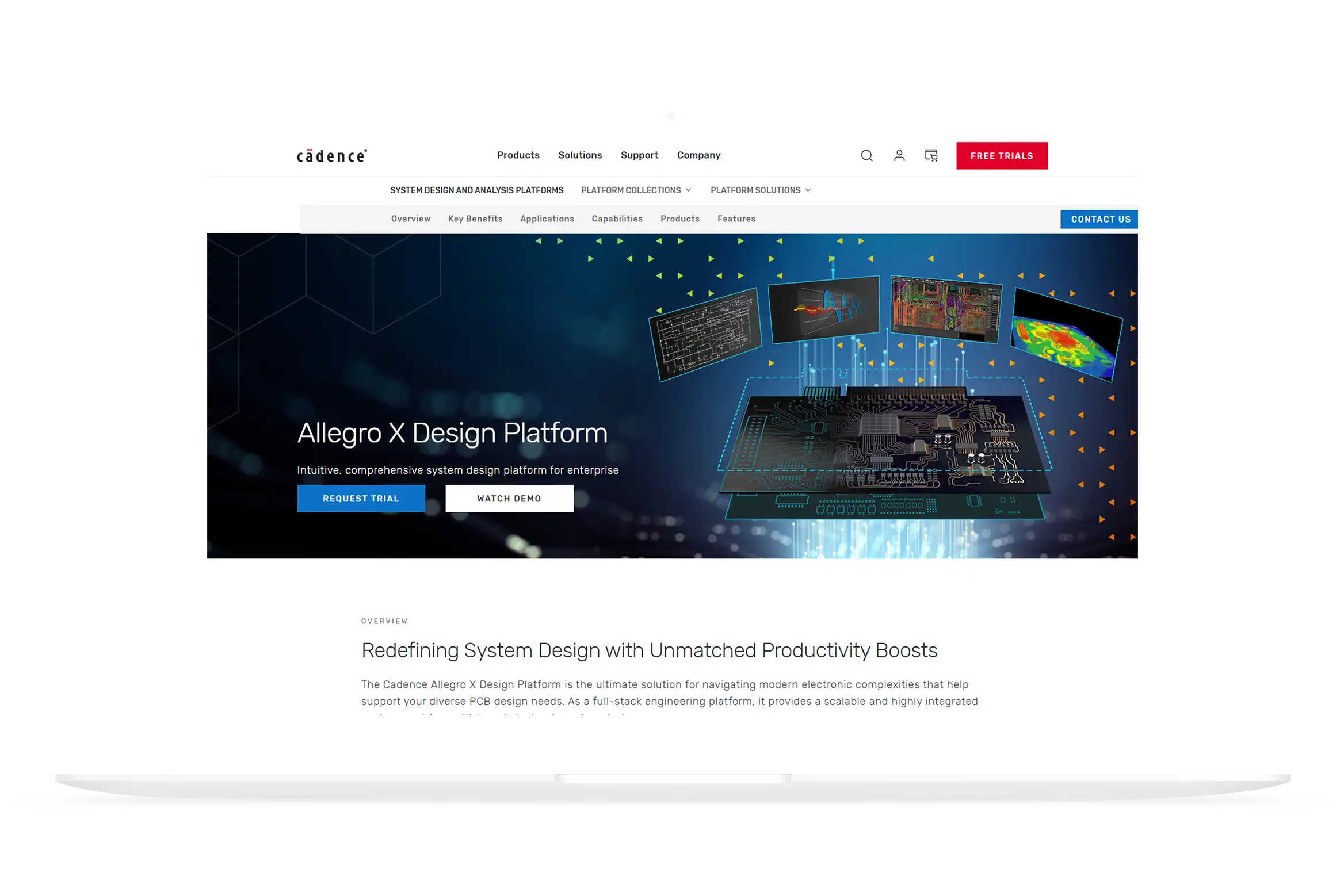
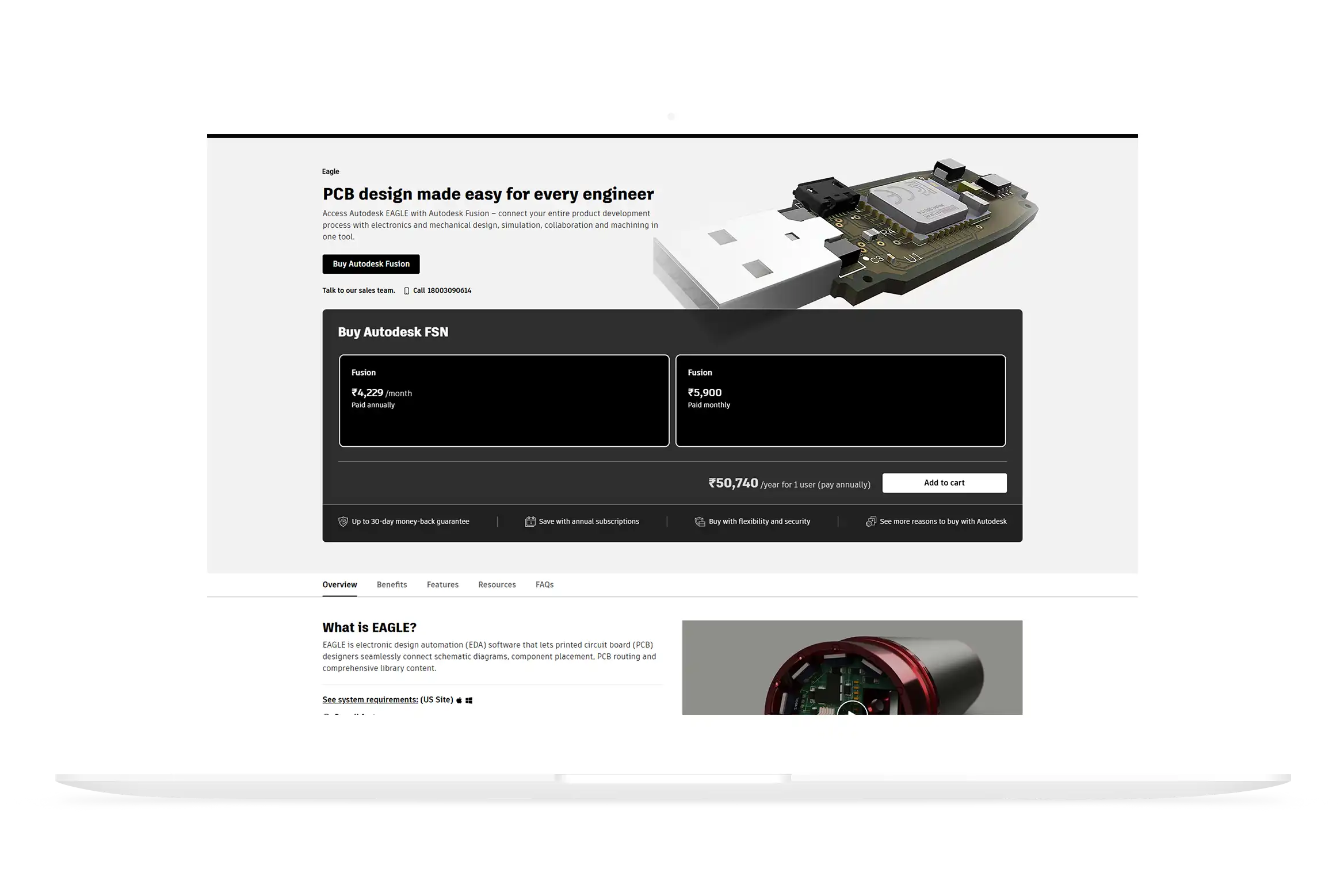
For PCB designing, we work on industry standard tools such as Altium Designer, KiCad, Cadence Allegro, and Eagle CAD to ensure each and every layout is DFM (Design for Manufacturability) compliant from day one.
If you need a rigid PCB, flexible PCB, or rigid-flex hybrid for a smart watch, a health patch, an equine wearable, or an industrial asset tracker, our engineers deliver precise schematics, optimized layouts, and validated prototypes ready for real-world deployment.
Get Free Quote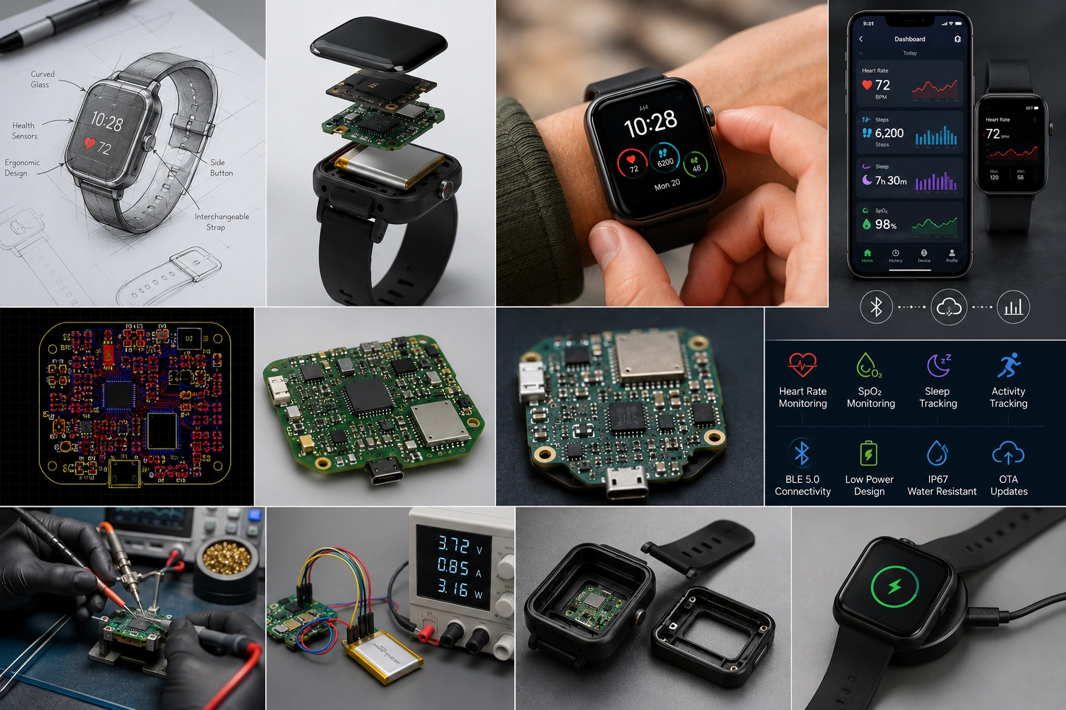
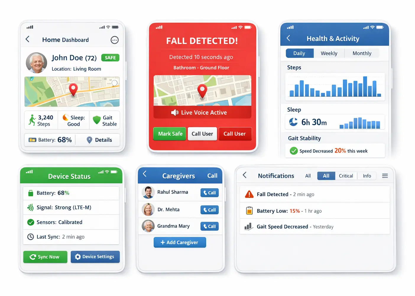
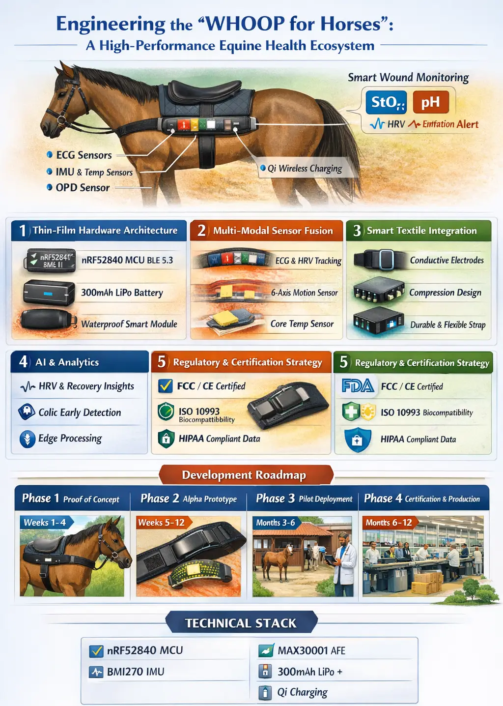
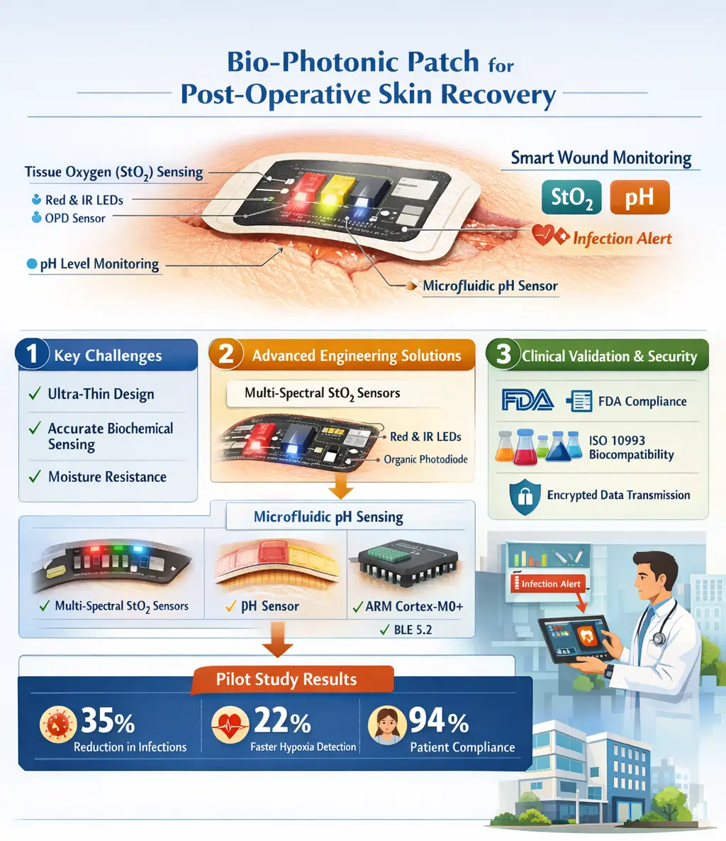
Real-World IoT Wearable Projects: Case Studies and Success Stories
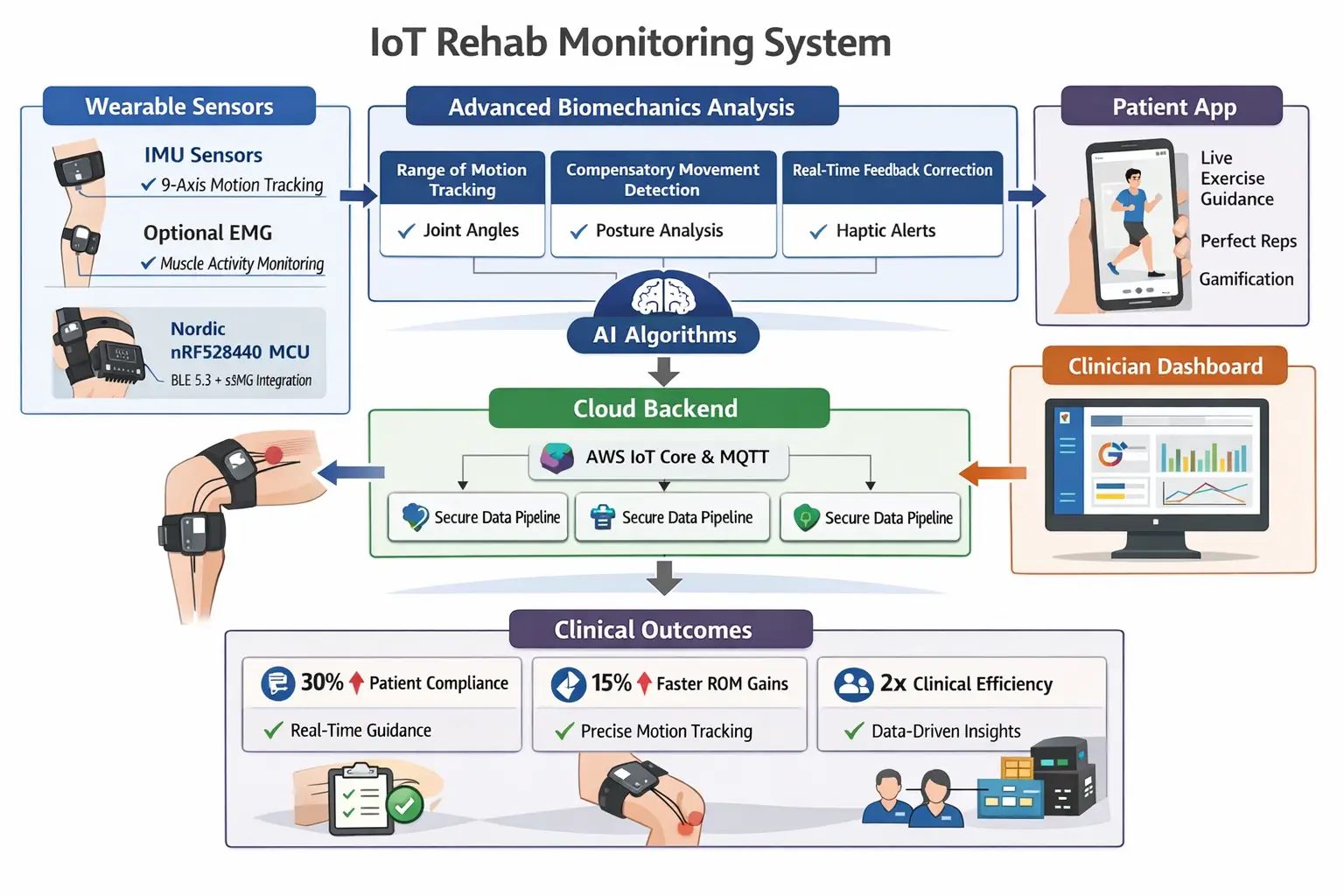
Explore some of our successfully delivered IoT wearable projects for global clients. We have provided custom IoT wearable solutions to a wide range of industries and businesses worldwide.
Discover how our hardware development expertise has helped clients achieve proven results through scalable innovation and reliable product development. We have also shared a case study from the industry, demonstrating our capability to work with different types of MCUs and showcasing our extensive experience in IoT wearable hardware development.
Our IoT Wearable PCB Design Services
1. Schematic Design & Capture
We start every project with a well-documented and clear schematic. Our engineers choose the right MCU, sensors, wireless module, power management IC and passive components based on your product power budget, size constraints and BOM cost targets.
We provide documentation for all component datasheets, reference designs and design decisions so your engineering team has complete traceability.
2. Layout and Routing Design for Wearable PCBs
Layout and Routing Design for Wearable PCBs is one of the more difficult areas of electronics engineering. Our Layout Design Engineers have extensive experience in providing the following types of designs:
HDI layouts (2 to 8 layers) to produce small form factor boards Trace Routing for 50Ω impedance control for RF signal integrity Quiet Ground Plane designs to minimize RF noise interference Trace Antenna (MWF) or Chip Antenna integration Mixed-Signal Isolation for analog biosensors Thermal Vias on Battery Chargers ICs and Power Regulators Placement of Components based on mechanical rigidity of the small form factor used in wearable applications.
3. Flexible PCBs (FPCB)
When designing PCBs for use in wearable devices that will be worn on the body, we will utilize flexible PCB technology using polyimide substrates (Kapton). Some of our design skill set in this area includes:
Single and double-sided flexible PCB design Bending radius analysis to prevent trace cracking Conformal coating for moisture and sweat resistance Low profile and lightweight designs for smart textiles, patches, and bands
4. Rigid-Flex PCB Design
For more complex wearable devices that need a combination of a rigid structure and flexible circuits, we design rigid-flex PCB boards.
By taking this approach we eliminate the need for connectors, resulting in fewer mechanical failure points, and create ultra-thin PCB profiles (5-8mm). Rigid-flex PCB applications include wearables for equine applications, clinical grade health patches, smart rings and advanced fitness trackers.
5. Rapid Prototyping & Validation
Speed to prototype is critical in wearable product development. Our process:
-
Gerber file generation and DFM review before sending to fabrication -
SMT assembly coordination with trusted PCB manufacturers -
Prototype bring-up: power sequencing checks, JTAG/SWD flashing, sensor validation -
Signal integrity testing and RF range testing -
Iteration cycle support until the hardware is validated
Why Companies Prefer Adequate Infosoft for Wearable PCB Design
Adequate Infosoft is an International IoT development firm that has expertise in designing applications for various industries such as Healthcare, Fitness, Agriculture and Manufacturing. Examples of our successful projects would be Wearable Audio Devices, Wearable Health Monitors, and Remote Patient Monitoring Systems to mention a few.
PCB design from schematic to layout to prototyping to production-ready PCBA Proficiency in ultra-miniature form factors (rings, patches, watch bands, under-5mm profiles) Focused on designing low power circuits to optimize battery life BLE, Wi-Fi, LoRa, Zigbee and cellular RF layout and antenna design Capability to design rigid, flexible & rigid-flex PCB HDI (High-Density Interconnect) 4–6 layer layouts for space constrained designs Designs compliant with CE, FCC, RoHS ready for regulatory submission Includes development of cloud firmware and companion mobile app
Take a video tour of our PCB manufacturing and embedded systems facility. From PCB design and firmware development to prototyping, assembly, testing, molding, and final product validation, we handle everything in-house.
Custom IoT Wearable PCB for Specific Platforms
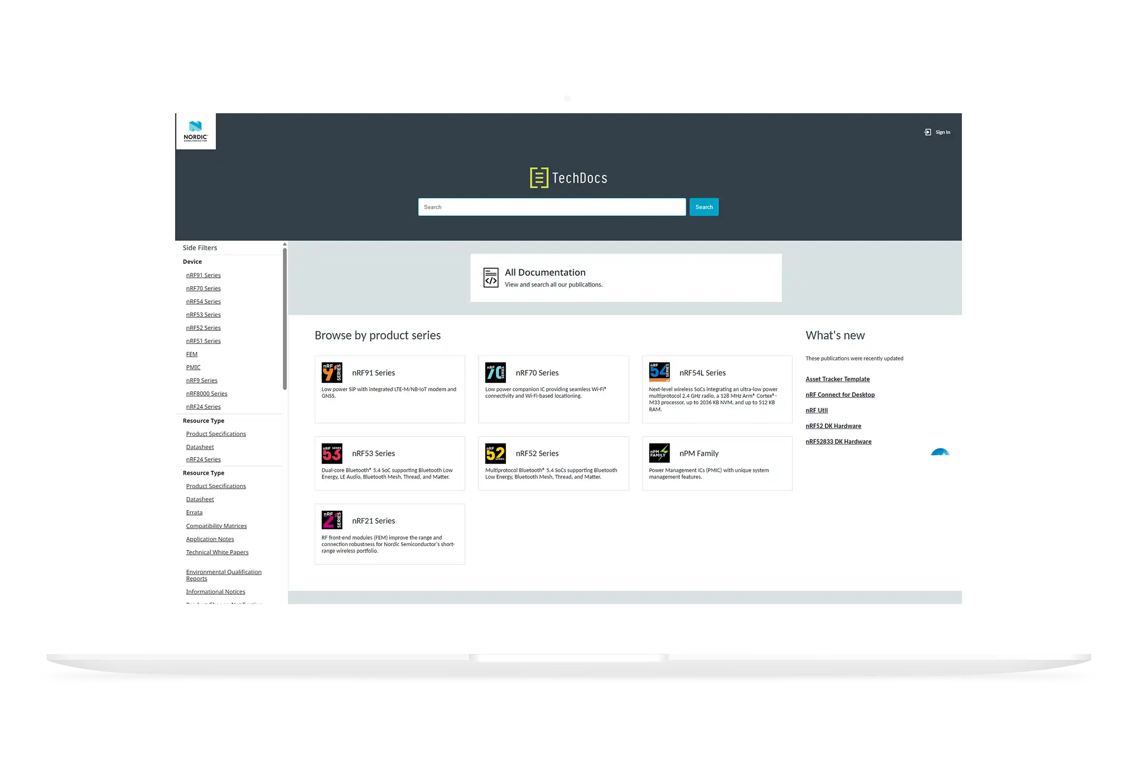
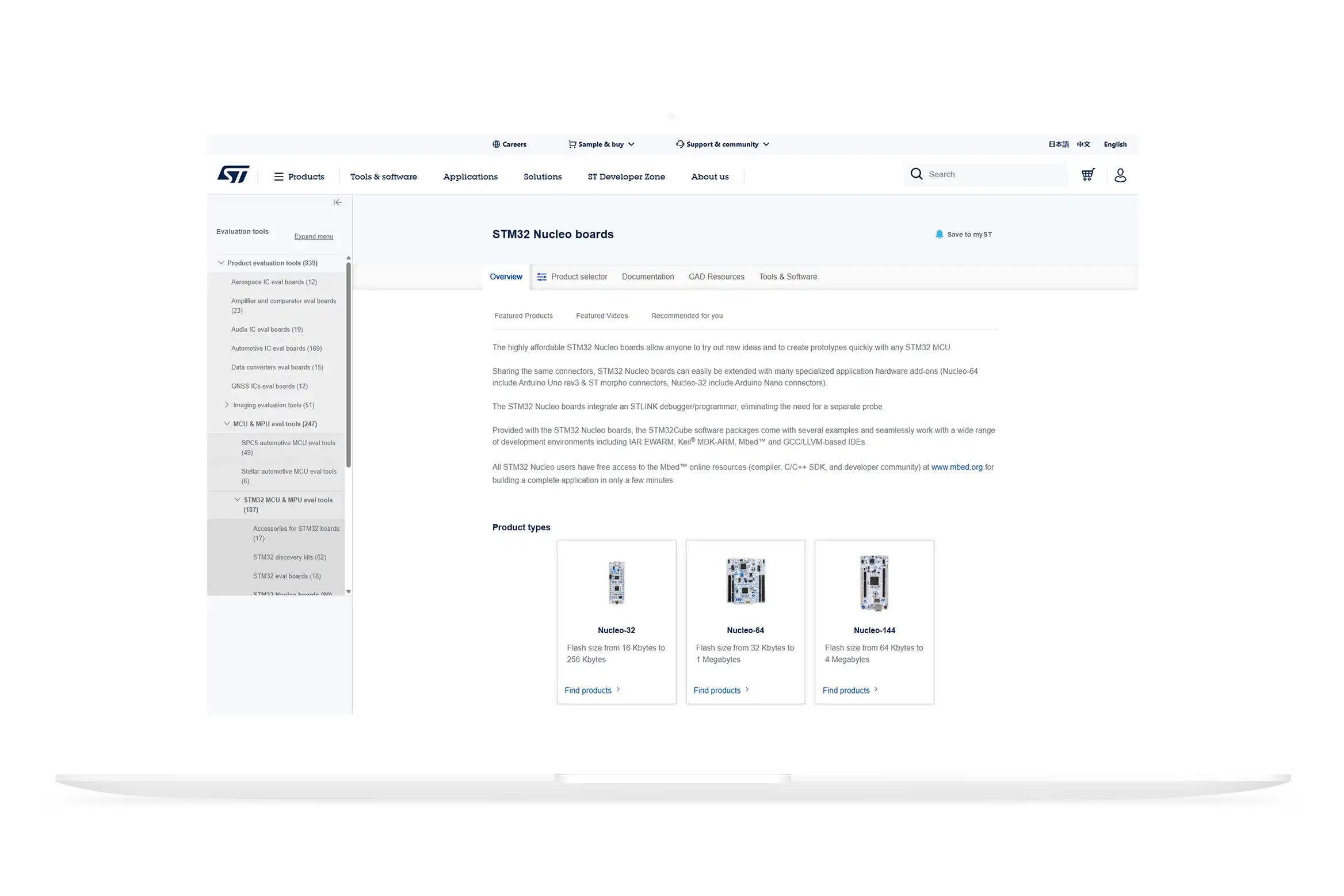
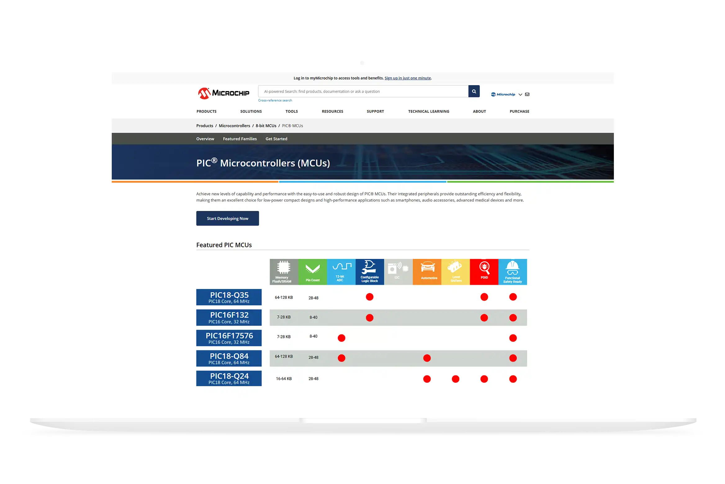
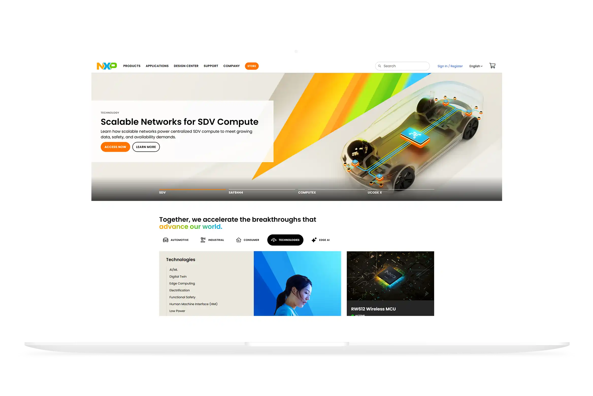
We design platform-specific PCBs optimized for the most popular IoT SoCs:

PCB Design Specifications We Work With
| Specification | Capability |
|---|---|
| Layer Count | 2 to 8 layers (HDI) |
| Min. Trace Width / Spacing | 3 mil / 3 mil |
| Board Materials | FR-4, Polyimide (Kapton), Rogers RO4350B, PTFE |
| PCB Type | Rigid, Flexible, Rigid-Flex |
| Surface Finish | HASL, ENIG, ENEPIG |
| Assembly | SMT, Through-hole, Mixed |
| RF Impedance Control | 50Ω (single-ended), 100Ω (differential) |
| Min. Package Size | 0201, 01005, µBGA, CSP, LGA |
| Wireless Protocols | BLE 5.x, Wi-Fi 802.11 b/g/n/ax, LoRa, Zigbee, Thread, Matter, NFC, UWB |
| Certifications Supported | FCC, CE, RoHS, IEC 60601 (medical), IP ratings |
Our PCB Prototyping Process (Step by Step)
Process for Creating a Printed Circuit Board Prototype, Step by Step
Step 1:
Requirements and Choosing Components. We will take a look at your Product Brief, establish critical performance requirements including; Power Budget, physical size of the product, and what type of connectivity is required, and establish which MCU, sensors, and wireless modules are best to use in your design based on our BOM Cost Analysis.
Step 2:
Schematic Capture - Complete schematic created in Altium Designer or KiCad. Includes all of the required sub-systems; Power Management, MCU, Sensors, Wireless, Charging Circuit, and I/O.
Step 3:
PCB Layout & DRC - Selection of Layer Stackup for PCB, Component Placement, Routing, Impedance Control and DRC and 3D Visualization of layout to be approved before sending to manufacturing.
Step 4:
DFM Review and Gerber Generation - Create DFM report with engineering recommendations to eliminate costly rework, increase yield, and eliminate manufacturing costs. Includes; Fiducial Markers, Tooling Holes, and Solder Mask Review.
Step 5:
Prototype Fabrication & Assembly - Send Gerber files to qualified PCB manufacturers. Coordinate SMT Stencil and Assembly with PCB manufacturer. 1st Article Inspection to be completed prior to Functional Testing.
Step 6:
Bring Up and Validation - Power On Testing, Flash Firmware, Calibrate Sensors, RF Range Testing, and Signal Integrity. Develop Final Test Report.
Step 7:
Iteration and Handoff to Production - Update Design based on Prototype Results. Deliver Final Production Ready Gerber Files, BOM and Assembly Documentation.
Tools We Use for PCB Design
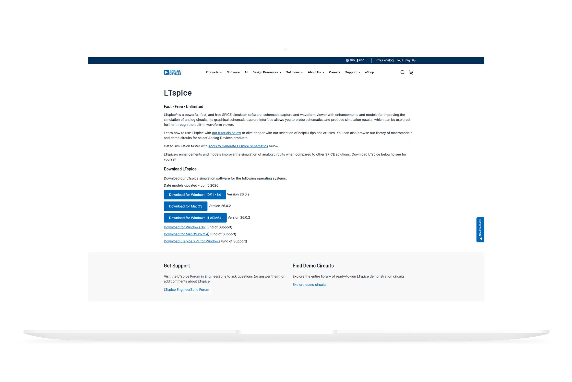
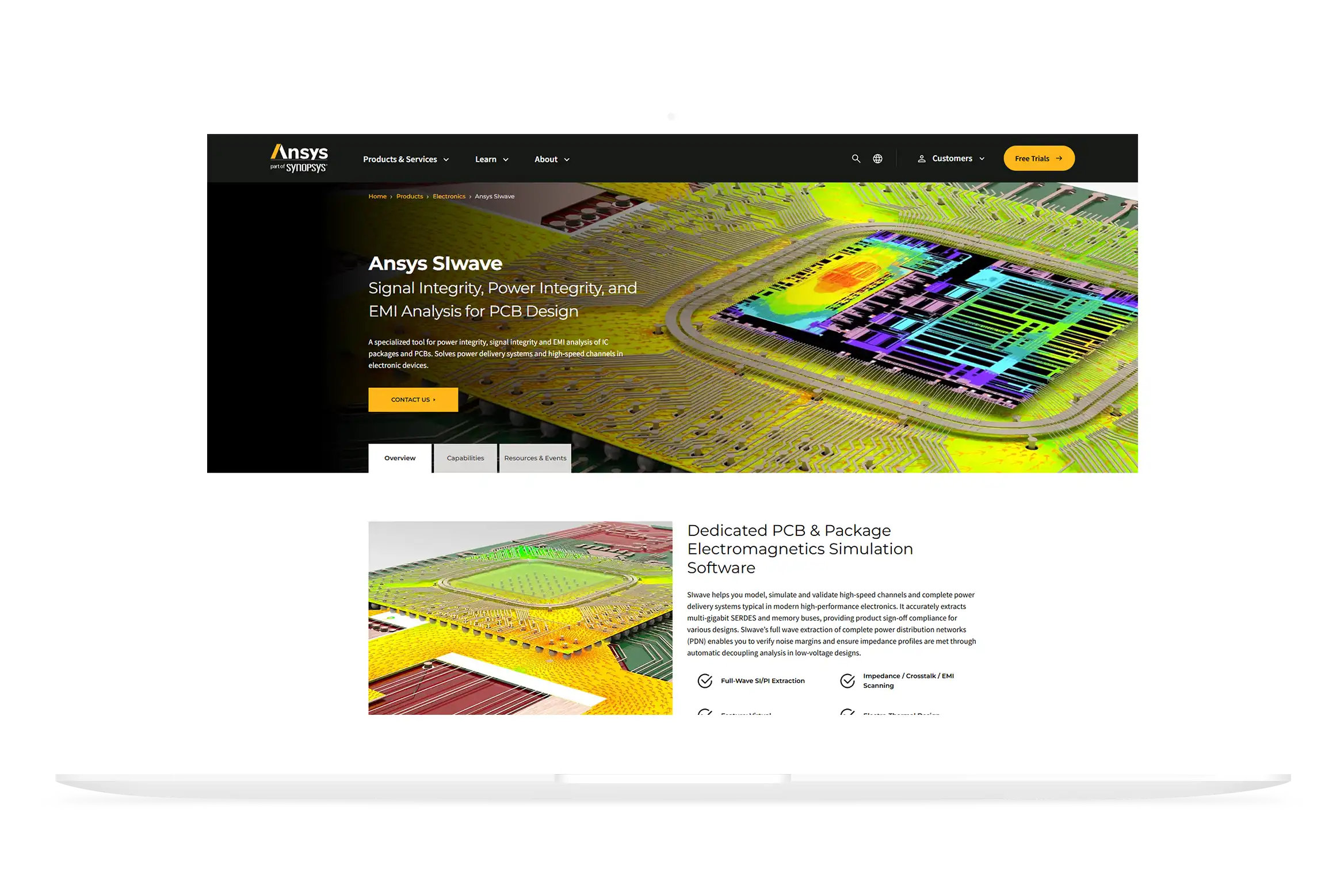
Our engineers have hands-on experience using the following widely accepted industry standard PCB EDA tools:
Frequently Asked Questions (FAQ)
The main PCB design tools used are Altium Designer and KiCad. But if you need signal integrity analysis for your project we can also use Cadence Allegro and HyperLynx. The choice of PCB design tools depends on the complexity of the project and the requirements of the customers.
Yes, Polyimide materials are used to manufacture flexible single and double layer PCBs. For an advanced wearable device that requires some structural support but still requires some flexibility, we can design a rigid-flex PCB.
We support BLE 5.x, Wi-Fi (802.11 b/g/n/ax), LoRa, Zigbee, Thread, Matter, NFC, UWB, and cellular (LTE-M/NB-IoT) for your wearable devices' connectivity requirements.
Yes! Adequate Infosoft is a complete IoT wearable device development company. We design and develop the PCB, write and debug the embedded firmware, develop the mobile app, and provide the cloud backend for your device as a single team.
Yes! All our PCB designs are created with compliance issues in mind, including the selection of RF modules including pre-certified modules, including techniques for providing EMI shielding techniques, and all of the documentation needed for FCC/CE submissions.
Time will vary with complexity level, but most projects will progress from initial schematic to validated prototype in approximately 6 to 12 weeks. Short end of that time frame would be typical simple two layer designs, but complex rigid/flex high density interconnect (HDI) prototypes could take longer.
Of course! Before we discuss any technical subject matter we will sign a Non-Disclosure Agreement so we understand the importance and treat all of our customer's Intellectual Property with the utmost confidentiality.
Yes, we do support small batch prototyping, usually 3-10 units, through full production ramp-up. We are always happy to work with you through all the stages of your product life cycle.
Technologies & Platforms
| Category | Technologies |
|---|---|
| Microcontrollers / SoCs | ESP32, ESP32-S3, nRF52832, nRF52840, nRF5340, STM32L4, STM32L5, STM32H7, NXP i.MX RT, Microchip PIC32, AVR, Silicon Labs EFR32, Renesas RA/RX |
| Wireless | BLE 5.x, Wi-Fi 802.11, LoRa, LoRaWAN, Zigbee, Thread, Matter, NFC, UWB, LTE-M, NB-IoT |
| PCB EDA Tools | Altium Designer, KiCad, Cadence Allegro, Eagle CAD, LTspice, HyperLynx |
| Sensors | PPG, ECG/AFE, SpO2, IMU (accelerometer + gyroscope + magnetometer), temperature, humidity, GPS/GNSS, flex, force, EDA, UV |
| Power Management | BQ25xxx series, MAX17xxx fuel gauges, LDO regulators, DC-DC buck/boost converters, wireless charging (Qi) |
| Cloud Platforms | AWS IoT Core, Azure IoT Hub, Google Cloud IoT, custom MQTT brokers |
| Firmware Frameworks | FreeRTOS, Zephyr RTOS, ESP-IDF, STM32CubeIDE, nRF Connect SDK, Arduino (prototyping) |
| Mobile | React Native, Flutter, iOS (Swift), Android (Kotlin) |
Certified IoT Hardware Development Experts
Our team includes certified professionals in AES security, Azure IoT, AWS Cloud, Google Cloud, and Microsoft architecture solutions. We provide secure and production ready IoT hardware development services with deep expertise in embedded hardware, IoT firmware, BLE/WiFi connectivity, cloud integration and scalable device ecosystems. Our certifications are not just words but backed by real industry experience, successful IoT deployments and verified credentials. You can check our certification proofs and technical expertise below.
Meet Our Global IPC-CID Certified PCB Design Team
Our worldwide team of IPC-Certified PCB Designers with the CID rating has many years of PCB design experience, including designing high-speed and multilayer PCBs, determining signal integrity, compliance to EMI/EMC guidelines, and providing manufacturing-ready solutions. We have designed PCBs for the following industries: medical; aerospace; industrial; consumer electronics; and telecommunications. Thus, our engineers provide reliable, high-quality PCB designs that help to increase product-development speed and ensure successful manufacturing.

Phil, UK
Certified Developer: PCB Design & Layout for EMC Compliance
PCB Design & Layout IPC Certified Interconnect Design Analog Circuit Design High-Speed PCB Design Mixed-Signal Design EMC/EMI-Compliant PCB Layout Altium Designer & Altium 365 Mentor PADS Zuken Cadstar PCB Manufacturing & DFM Signal Integrity Power Integrity Audio Electronics Design Hardware Development Electronic Product Design

C.I.D. Certified Interconnect Designer Certified Face Recognition Application using Python 17+ Years PCB Design Experience Multilayer PCB Design (Up to 32 Layers) High-Speed & Mixed-Signal Design HDI, Rigid-Flex & FPC Boards DDR, PCIe, Ethernet & RF Layouts FPGA & Processor Board Design EMI/EMC, DFM, DFA & DFT Expertise PCB Stack-Up & Signal Integrity PCB Manufacturing & CAM Review Library Creation & Component Engineering

Engineer Printed Circuit Board Designer Excellence Awards Signal Integrity: Fundamentals to Advanced with Simulations Certificate PCB Design & Hardware Development Circuit Design & Schematic Capture PCB Layout & Routing Altium Designer Gerber Generation & Manufacturing Support Component Selection & Engineering EMI/EMC Compliance Hardware Scaling & Optimization

Certified Interconnect Designer (Credential ID CID-23102549900) IPC Certified PCB Designer Senior Hardware Design Engineer R&D Hardware Development PCB Design & Layout High-Speed & Multilayer PCB Design EMI/EMC-Compliant Design Hardware Validation & Testing

PC-CID Certified Interconnect Designer PCB Design & Layout Engineering Schematic Design & Development Altium Designer & Camtastic Multilayer PCB Design & DFM ATE DUT Board & Motherboard Design EMI/EMC Compliance & Validation

Electronic Engineering PCB Design & Layout IPC-CID Certified Interconnect Designer MInstCT (Institute of Circuit Technology) Member Quality Assurance Safety & Compliance Standards X-Ray Tube Assembly Manufacturing & Process Engineering Life Cycle Assessment – Foundation Six Sigma and Lean: Foundations and Principles (Credential ID 106904317)