


 Mean Stack Development
 Vue JS Development
 Javascript Development
 React JS Development
 Angular JS Development
 Next JS development
 Java Development
 Python Development
 Django Development
 Cherrypy Development
 C# Development
 ASP.NET Development
 NodeJS Development
 Laravel Development
 CodeIgniter Development
 Zend Development
 Ruby on Rails Development
 CakePHP Development
 PHP Website Development
 Symfony Development
 Drupal Development
 Joomla Development
 Wordpress Development
 .NET Nuke Development
 Kentico
 Umbraco
 .NET MAUI Development
 Xamarin Application Development
 iOS Application Development
 Android Application Development
 Android Wear App Development
 Ionic Development
 iBeacon Application Development
 Universal Windows Platform (UWP)
 Kotlin Application Development
 Swift Application Development
 Flutter Application Development
 PWA Application Development
 Flutter Health Tech & Wearable App Development Company
 React Native Health Tech Wearable App Development
 Offshore Software Development
 Custom Application Development
 Front-End Development
 Full Stack Development
 AI & Machine Learning
 Custom CRM Solutions
 Flask Software Development
 Electron JS Development
 ChatGPT Development
 Telemedicine App Development
 Build Smart Telemedicine Platform
 Beauty & Salon App Solutions
 Hire Workato Experts
 Magento Development
 Magento 2.0 Development
 Magento Enterprise
 Shopping Cart Development
 Prestashop Development
 Shopify Development
 Open Cart Development
 WooCommerce Development
 BigCommerce Development
 NopCommerce Development
 Virto Commerce Development
 AspDotNetStorefront Development
 .NET Application Development
 Microsoft Dynamics CRM
 VB .NET Development
 Sharepoint Migration
 ASP.NET Core Development
 ASP.NET MVC Development
 AJAX Development
 Agile Development
 Microsoft Bot
 Microsoft Blazor
 Microsoft Azure Cognitive
 HTML 5
 UI/UX Design
 Graphic Design
 Adobe Photoshop
 XML Application Development
 Cloud Computing Solutions
 Azure Cloud App Development
 AWS Development
 Google Cloud Development
 Certified AWS IoT Services Developers
 DevOps Consulting & Development
 Kubernetes Consulting & Services
 SQL Programming Development
 MySQL Development
 MongoDB Development
 Big Data
 Robotic Process Automation
 Social Media Marketing
 Search Engine Optimization
 QA Testing
 Software Testing
 Software Security
 Maintenance And Support
 I.T. Consulting Services
 Business Intelligence
 YII Development
 Data Analysis
 Alexa Skills Development
 On Demand App for Mobile repairing services
 On Demand App for Car Service Booking
 On Demand App for Cleaning Services
 On Demand App for Pharmacy
 On Demand Dedicated Developers
 On Demand Lawyer App Development












 Nuki Smart Lock
 Salto Smart Lock
 TTlock Smart Lock
 NFC App Development
 Custom IOT Enabled Smart Lock
 Smart Locker Solutions
 Hospital Smart Lock Systems
 Hotel Smart Lock Systems
 Smart Home & Office Locks
 Smart Access for Schools & Colleges
 Unloc Smart Lock Integration
 Yale & August Smart Lock Integration
 Populife Smart Lock Integration
 Smart Lock Hardware Development
 Dairy IoT Solutions
 Agri IoT & AI Solutions
 Weather & Climate Solutions
 Water & Waste Management Solutions
 RaspBerry Pi
 Firmware Software Development
 ESP 32 Software Development
 Embedded Development
 Internet of Things
 Smart IoT Development
 IoT Sensor Integration & Development Solutions
 Smart IoT System Development for HVAC
 Tuya IoT App Development
 Particle IoT SDK
 IoT Development with AI
 Smart Pet GPS Tracker
 Dairy GPS Tracking Solutions
 GPS Fleet Management Software
 Car Rental & Subscription Solutions
 Car Buy & Sell Marketplace Development
 AI-Powered Car Wash App Development
 PCB Design & Fabrication
 IoT AC Automation
 AI–IoT Painting Solutions
 IoT Wearable Hardware & App Development
 HVAC Automation & AI Control Systems
 Smart Home IoT Engineering
 AI Embedded Systems
 AI Hardware Design Service
 Advanced IoT Hardware & Firmware Development
 Device Driver Development Services
 NXP i.MX RT Firmware & Hardware Services
 Microchip PIC & AVR Development
 Hire IoT Architects
 IoT Cloud & Infrastructure Solutions
 Infineon XMC / AURIX Development Services
 Matter & Thread IoT Services
 Native IoT Mobile App Development (BLE & Wi-Fi)
 Snapdragon IoT Firmware Development
 Renesas RA/RX Firmware Services
 Silicon Labs EFR32 Development Services
 Smart Wearable App Development
 Smart IoT Meters
 Smart Healthcare Wearable App Development
 Health Care Monitoring System
 Fitness Tracking App Development
 Smart Home Automation Apps
 nRF PCB Design
 ESP32 PCB Design
 Embedded Wearables Engineers
 Rental Property Management System
 Building Management System
 Smart Lighting Development
 Infineon Semiconductor Firmware Development Services
 Custom Camera Development: Hardware, Firmware & PCB Prototyping
 Smart Security Camera SDK
 Nordic Semiconductor SDK
 Infineon SDK
 Arduino SDK
 NFC Lock Integration
 Kerong Lock Integration
 IoT & AI Solutions for Manufacturing
 Smart Inventory & Logistics Solution
 Food & Beverage Industry Solutions
 Smart Hospitality Solutions
 Smart Property Management
 Custom Smart Home IOT SDK
 Smart IoT & AI in Healthcare
 AI-Powered Security Solutions
 Smart Home Safety & AI
 Veterinary Clinic Management (AI)
 Pet Care System (AI & IoT)
 Pet Training & Adoption (AI)
 Healthcare IoT Development
 Event Management Software
 Money Remittance App
 Money Lending App Development
 Utility and Bill Payment App
 IoT Mobile App Development (Flutter & React Native)
 AI & IoT Retail Solutions
 Smart EV App Development
 Smart Solar IoT & AI Solutions
 IoT-Based Energy Systems
 Smart Energy & Utilities Solutions
 6G Solutions
 IoT Security Solutions
 AI-Powered Lottery App Development
 AI-Sports Fitness Club Management
 Travel
 Real Estate
 Medical & Healthcare
 e-Learning
 Consumer Products
 Finance
 Automobile
 Media & Entertainment
 Billing Software
 Enterprise Resource Planning (ERP)
 Augumented & Virtual Reality
 Point of Sale(POS) Development
 Learning Management System
 EV Charging Solutions
 About Us
 Partners & Certifications
 Quality Assurance
 Our Clients & Testimonials
 Development Process
 Our Products
 Social Responsibility
 Work Ethics
 Vision & Mission
 Awards
 Live Project Demos
 Contact Us
 Case Studies
 Portfolio
 Blog
RF and Wireless PCB Design Services for Connected Products
A wireless solution is able to perform well on a development board, and then face huge problems with the real-life implementation. Bluetooth connectivity may work coherently. Wi-Fi transmission may even create resets.
Devices may work flawlessly on a test bench but may fail to send some data when placed by industrial machines.
Adequate Infosoft provides RF and wireless PCB design services for connected sensors, wearables, smart locks, industrial monitoring devices, and IoT products. Our published work includes custom boards built around Nordic, Espressif, and Silicon Labs wireless platforms.
Our focus is practical: help product teams develop hardware that communicates reliably, supports manufacturing, and comes with the documentation needed for future production and maintenance.
Let's Work Together!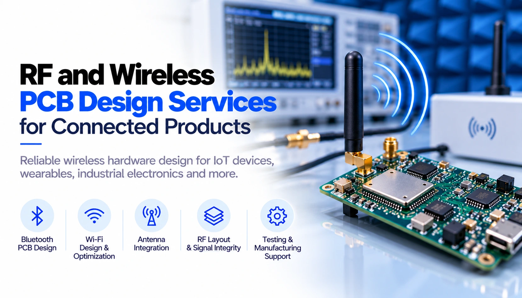
What Does RF and Wireless PCB Design Include?
The design of RF PCB entails placing and routing the radio circuits, antennas connections, matching elements, power supply, and supporting electronics.
The manufacture of wireless PCB takes it further into the complete connected device, which has sensors, charging circuits, programing interfaces, and production testing equipment.
A proper design takes into consideration the frequency band, casing, installation environment, the needs of batteries selected, and methods of production right from the start of the process.
Controlled-Impedance Routing and PCB Stack-Up Planning
Impedance that is suitable for radio frequency design is required from the transmission line, which is mostly 50 ohm at the matching points. Trace width by itself does not give the impedance as dielectric thickness, copper shape, material characteristics, and the reference plane also play a role in determining the impedance.
We plan routing around the fabricator's proposed stack-up. Critical RF connections need short paths, suitable grounding, and carefully managed transitions.
Four-layer construction can improve routing and reference-plane continuity, but layer count should follow the actual electrical and mechanical requirements.
RF Antenna Placement and Matching
The antenna must have room to work. Parts such as batteries, metal parts, display, cables, and enclosure material influence its performance.
Thus, make sure to choose the antennas while doing the mechanical design. PCB antennas, chip antennas, module antennas, and external antennas may have different interference and grounding requirements. The keep-out areas must comply with the information provided by the manufacturer.
For a custom RF path, provision for matching components allows prototype tuning. An antenna match measured on an exposed board should also be checked in the assembled product; impedance matching alone does not prove good radiated performance.
Signal Integrity, Power Integrity, and Thermal Management
The requirements of wireless transmission will lead to changing current demands. The lack of proper regulation or decoupling may result in voltage dips, instability in measurements, and unwanted resets.
In our design review we will pay attention to power paths, return currents, locations of switches and sensors, and some distance between noise-generating and sensitive circuits.
Thermal management also matters around charging circuits, regulators, and higher-power transmitters, particularly inside sealed enclosures.
EMI and EMC Risk Reduction
EMI and EMC issues may arise once a prototype is submitted for certification testing even if it was functioning well prior to compliance testing.
PCB design should rationally address the fixed paths of switching, routing of the clock signals, connecting interfaces and ground layout as well as design for ESD protection. Using pre-compliance measurements allows for catching possible incompatibility before compliance testing starts.
Different certification requirements apply to different products and markets; reviewing a design might not guarantee compliance with regulations.
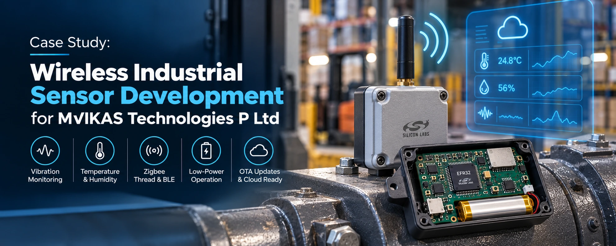
Case Study: Wireless Industrial Sensor Development for MVIKAS Technologies P Ltd
The Client and Operational Challenge
Adequate Infosoft's published industrial sensor case study identifies the client as MVIKAS Technologies P Ltd, a company working in warehouse automation.
The client wanted superior visibility in terms of machinery and environmental conditions at distribution sites. The current monitoring solution used at that time was scattered and thus, it was challenging to consolidate operating data and apply predictive maintenance.
The project required connected sensing hardware supported by firmware, cloud services, and applications. Wireless communication was central to that requirement: measurements had to become useful operational information rather than remain isolated at individual machines.
Documented Hardware and Software Delivery
The published implementation makes mention of custom multilayer PCB made of Silicon Labs EFR32 wireless SoC which can monitor vibrations along with temperature and humidity.
The solution implemented different battery management systems, low energy operation as well as industrial casing. The various technologies being utilized in the device include Zigbee, Thread, and BLE. Furthermore, it supports OTA updates along with local processing in firmware.
The manufacturing section also describes functional testing of sensors, power consumption, wireless operation, and update capabilities, together with automated flashing and calibration. This establishes relevant experience across board development, embedded software, and device preparation.
RF Engineering Lessons for Similar Industrial Products
In developing similar devices, the key engineering lesson for the buyers is determining radio functionality together with sensing and power performance. The technical implications of this architecture are explained in the next points; these points are not fabricated claims about the measurements of the project not yet published.
A vibration sensor can generate frequent data transfers while a wireless transmitter draws short current pulses. If the supply or return path is poorly arranged, communication activity may disturb acquisition or create intermittent faults. Prototype evaluation should therefore exercise sensing and transmission together.
Antenna position also needs to reflect the installation. A unit mounted beside a steel cabinet or motor may behave differently from the same device sitting on a laboratory table. Testing representative orientations and mounting conditions provides more useful evidence than a single open-air range demonstration.
Low-power operation introduces another trade-off. Longer sleep periods can conserve energy, but reporting frequency, reconnection behavior, and maintenance requirements still need to meet the customer's operational expectations.
What This Means for Production Planning
An industrial wireless circuit board should be manufactured so that the factory is able to detect faults reliably. Programming interfaces, measurable voltages, and repeatable tests of function all contribute to an easy diagnosis process.
An efficient testing process enables assembly faults to be differentiated from firmware, sensor, and RF faults. Identification of the device and recorded results would subsequently link the problems faced in the field with hardware revisions and production lots.
Why This Project Matters
The MVIKAS project demonstrates documented experience connecting custom wireless hardware with firmware and an operational monitoring platform.
For an RF PCB buyer, that matters because board performance affects the complete product. Stable communication, clean measurements, serviceable firmware, and repeatable manufacturing need to be considered together. Exact range, impedance tolerances, and production yield should still be established through project-specific requirements and test evidence.
Relevant Projects That Demonstrate Our Experience
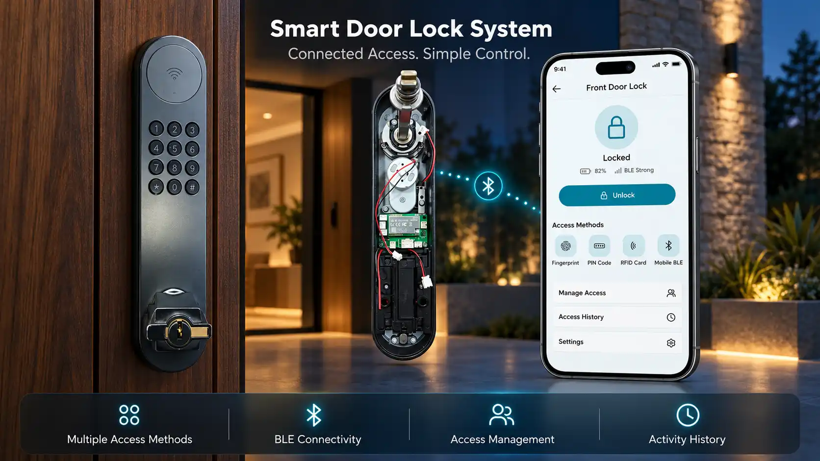
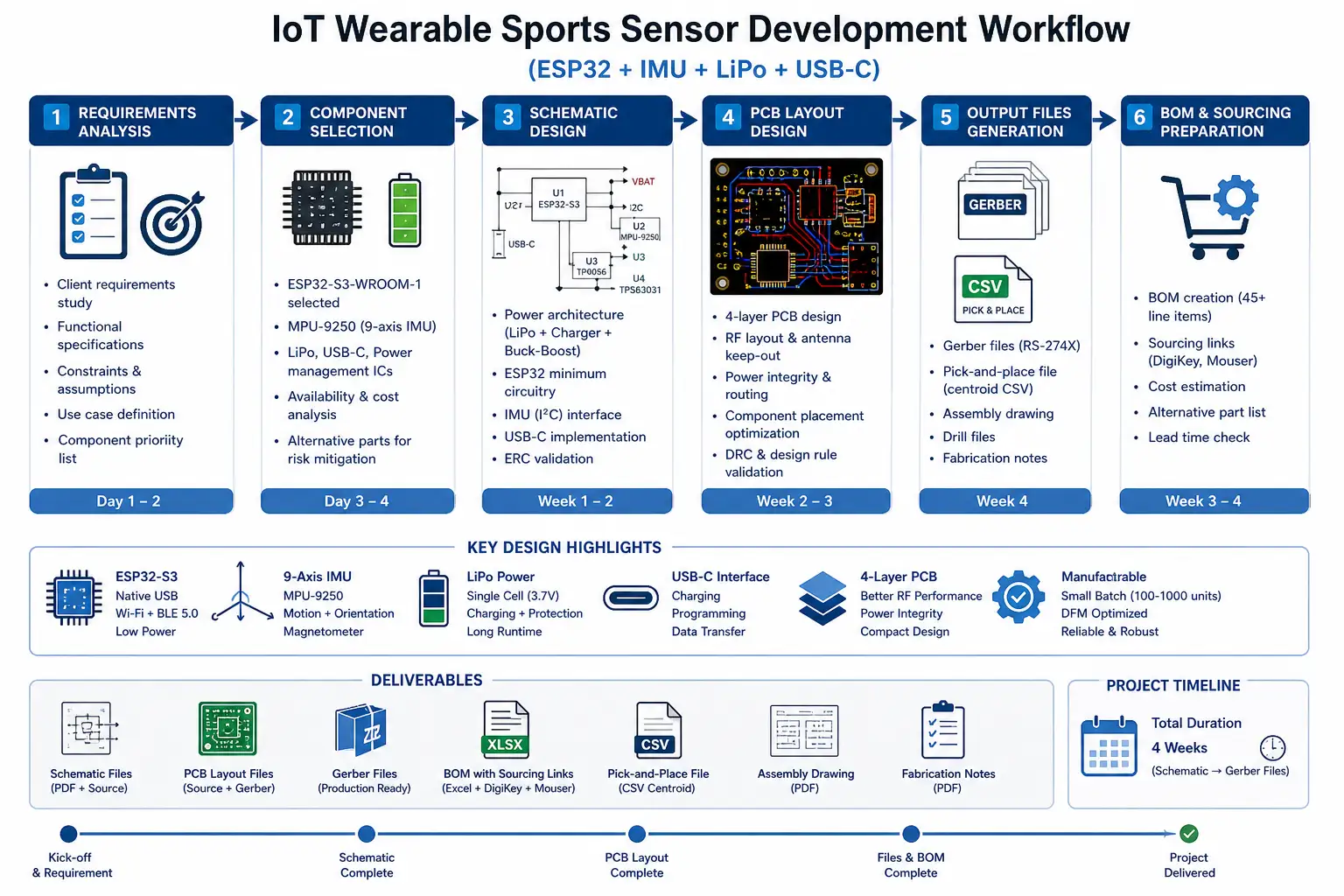
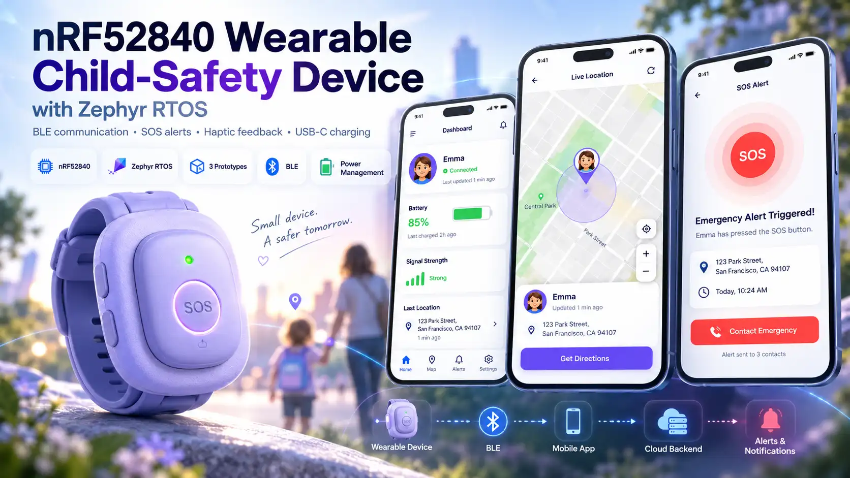
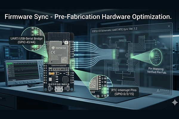
Our experience is supported by published project descriptions covering different wireless hardware constraints. These examples show the work delivered and its relevance to RF PCB development.
Designed for Manufacturing, Testing, and Ownership
Professional PCB buyers have additional requirements that go beyond a PCB. These obligations must be established before the layout starts.
Component availability
Here it is necessary to check the status of components in terms of lifecycle, availability at supplier's stock, terms for obtaining them, and possible risks in sourcing. In case of using alternative components, electrical, mechanical, and firmware verifications should be performed prior to their approval.
DFM and DFT
Design for manufacturing takes into consideration all limitations related to production and assembly processes. Meanwhile, design for testing makes sure that the essential process can be checked and malfunctions diagnosed.
Accessibility of testing points
It is important to have easy access to signals for programming, bus voltages, reset lines, and needed interfaces that are planned to be used.
Factory programming
Define firmware loading, device identifiers, credential provisioning, verification, and failed-unit handling. These steps should be repeatable and documented.
Production yield
Pilot builds should record defects, rework, and test failures. Yield improvements need evidence from production rather than assumptions based on a successful prototype.
Design-file Ownership Completion
The contract must outline ownership and transfer terms. Deliverables must clarify the editable design, PCB files, libraries, manufacturing results, BOMs, assembly plans, and testing documents with third-party usage license specified.
Discuss Your RF and Wireless PCB Project
When designing a small wearable, industrial sensor, or connected access control device, it is essential to identify all the criteria that the hardware must meet.
Adequate Infosoft can help you convert these criteria into a PCB development scope containing wireless integration, prototyping, manufacturing preparations, and delivered documentation.
Frequently Asked Questions
Using a module may ease the task of designing the solution and minimize some RF integration work. On the other hand, creating a custom circuit may offer more control over the cost and size of the solution compared to using the module. This choice depends on the pricing scheme, available resources, certification plan, and production volume.
Yes. Investigation should consider antenna clearance, matching, supply stability, grounding, enclosure effects, and firmware behavior. Measurements help determine whether the solution requires tuning, layout changes, or both.
It is important to provide information about the wireless protocol, target market, characteristics of enclosure, power supply, estimated manufacturing volume, working conditions, and design files. Be sure to provide measurable standards for acceptance testing whenever possible.
Editorial References