


 Mean Stack Development
 Vue JS Development
 Javascript Development
 React JS Development
 Angular JS Development
 Next JS development
 Java Development
 Python Development
 Django Development
 Cherrypy Development
 C# Development
 ASP.NET Development
 NodeJS Development
 Laravel Development
 CodeIgniter Development
 Zend Development
 Ruby on Rails Development
 CakePHP Development
 PHP Website Development
 Symfony Development
 Drupal Development
 Joomla Development
 Wordpress Development
 .NET Nuke Development
 Kentico
 Umbraco
 .NET MAUI Development
 Xamarin Application Development
 iOS Application Development
 Android Application Development
 Android Wear App Development
 Ionic Development
 iBeacon Application Development
 Universal Windows Platform (UWP)
 Kotlin Application Development
 Swift Application Development
 Flutter Application Development
 PWA Application Development
 Flutter Health Tech & Wearable App Development Company
 React Native Health Tech Wearable App Development
 Offshore Software Development
 Custom Application Development
 Front-End Development
 Full Stack Development
 AI & Machine Learning
 Custom CRM Solutions
 Flask Software Development
 Electron JS Development
 ChatGPT Development
 Telemedicine App Development
 Build Smart Telemedicine Platform
 Beauty & Salon App Solutions
 Hire Workato Experts
 Magento Development
 Magento 2.0 Development
 Magento Enterprise
 Shopping Cart Development
 Prestashop Development
 Shopify Development
 Open Cart Development
 WooCommerce Development
 BigCommerce Development
 NopCommerce Development
 Virto Commerce Development
 AspDotNetStorefront Development
 .NET Application Development
 Microsoft Dynamics CRM
 VB .NET Development
 Sharepoint Migration
 ASP.NET Core Development
 ASP.NET MVC Development
 AJAX Development
 Agile Development
 Microsoft Bot
 Microsoft Blazor
 Microsoft Azure Cognitive
 HTML 5
 UI/UX Design
 Graphic Design
 Adobe Photoshop
 XML Application Development
 Cloud Computing Solutions
 Azure Cloud App Development
 AWS Development
 Google Cloud Development
 Certified AWS IoT Services Developers
 DevOps Consulting & Development
 Kubernetes Consulting & Services
 SQL Programming Development
 MySQL Development
 MongoDB Development
 Big Data
 Robotic Process Automation
 Social Media Marketing
 Search Engine Optimization
 QA Testing
 Software Testing
 Software Security
 Maintenance And Support
 I.T. Consulting Services
 Business Intelligence
 YII Development
 Data Analysis
 Alexa Skills Development
 On Demand App for Mobile repairing services
 On Demand App for Car Service Booking
 On Demand App for Cleaning Services
 On Demand App for Pharmacy
 On Demand Dedicated Developers
 On Demand Lawyer App Development











 Nuki Smart Lock
 Salto Smart Lock
 TTlock Smart Lock
 NFC App Development
 Custom IOT Enabled Smart Lock
 Smart Locker Solutions
 Hospital Smart Lock Systems
 Hotel Smart Lock Systems
 Smart Home & Office Locks
 Smart Access for Schools & Colleges
 Unloc Smart Lock Integration
 Yale & August Smart Lock Integration
 Populife Smart Lock Integration
 Smart Lock Hardware Development
 Dairy IoT Solutions
 Agri IoT & AI Solutions
 Weather & Climate Solutions
 Water & Waste Management Solutions
 RaspBerry Pi
 Firmware Software Development
 ESP 32 Software Development
 Embedded Development
 Internet of Things
 Smart IoT Development
 IoT Sensor Integration & Development Solutions
 Smart IoT System Development for HVAC
 Tuya IoT App Development
 Particle IoT SDK
 IoT Development with AI
 Smart Pet GPS Tracker
 Dairy GPS Tracking Solutions
 GPS Fleet Management Software
 Car Rental & Subscription Solutions
 Car Buy & Sell Marketplace Development
 AI-Powered Car Wash App Development
 PCB Design & Fabrication
 IoT AC Automation
 AI–IoT Painting Solutions
 IoT Wearable Hardware & App Development
 HVAC Automation & AI Control Systems
 Smart Home IoT Engineering
 AI Embedded Systems
 AI Hardware Design Service
 Advanced IoT Hardware & Firmware Development
 Device Driver Development Services
 NXP i.MX RT Firmware & Hardware Services
 Microchip PIC & AVR Development
 Hire IoT Architects
 IoT Cloud & Infrastructure Solutions
 Infineon XMC / AURIX Development Services
 Matter & Thread IoT Services
 Native IoT Mobile App Development (BLE & Wi-Fi)
 Snapdragon IoT Firmware Development
 Renesas RA/RX Firmware Services
 Silicon Labs EFR32 Development Services
 Smart Wearable App Development
 Smart IoT Meters
 Smart Healthcare Wearable App Development
 Health Care Monitoring System
 Fitness Tracking App Development
 Smart Home Automation Apps
 nRF PCB Design
 ESP32 PCB Design
 Embedded Wearables Engineers
 Rental Property Management System
 Building Management System
 Smart Lighting Development
 Infineon Semiconductor Firmware Development Services
 Custom Camera Development: Hardware, Firmware & PCB Prototyping
 Smart Security Camera SDK
 Nordic Semiconductor SDK
 Infineon SDK
 Arduino SDK
 NFC Lock Integration
 Kerong Lock Integration
 IoT & AI Solutions for Manufacturing
 Smart Inventory & Logistics Solution
 Food & Beverage Industry Solutions
 Smart Hospitality Solutions
 Smart Property Management
 Custom Smart Home IOT SDK
 Smart IoT & AI in Healthcare
 AI-Powered Security Solutions
 Smart Home Safety & AI
 Veterinary Clinic Management (AI)
 Pet Care System (AI & IoT)
 Pet Training & Adoption (AI)
 Healthcare IoT Development
 Event Management Software
 Money Remittance App
 Money Lending App Development
 Utility and Bill Payment App
 IoT Mobile App Development (Flutter & React Native)
 AI & IoT Retail Solutions
 Smart EV App Development
 Smart Solar IoT & AI Solutions
 IoT-Based Energy Systems
 Smart Energy & Utilities Solutions
 6G Solutions
 IoT Security Solutions
 AI-Powered Lottery App Development
 AI-Sports Fitness Club Management
 Travel
 Real Estate
 Medical & Healthcare
 e-Learning
 Consumer Products
 Finance
 Automobile
 Media & Entertainment
 Billing Software
 Enterprise Resource Planning (ERP)
 Augumented & Virtual Reality
 Point of Sale(POS) Development
 Learning Management System
 EV Charging Solutions
 About Us
 Partners & Certifications
 Quality Assurance
 Our Clients & Testimonials
 Development Process
 Our Products
 Social Responsibility
 Work Ethics
 Vision & Mission
 Awards
 Live Project Demos
 Contact Us
 Case Studies
 Portfolio
 Blog
PCB Redesign, Re-spin & Component Obsolescence Engineering Services
A PCB does not always need to be replaced because it is fundamentally bad. Sometimes it has one power rail that collapses under load, one unavailable component holding up production, or one interface that becomes unreliable after the board enters its enclosure. The difficult part is finding that issue without creating five new ones.
Adequate Infosoft specializes in PCB redesign, board re-spin, and component obsolescence services for startups, original equipment manufacturers (OEMs), and production companies that have an already produced or almost perfect hardware.
We diagnose the problems, analyze the existing design, make necessary modifications to the affected areas, and help the revised board to reach the stage of prototyping and production.
Our engineers work in the sphere of embedded controllers, wireless devices, industrial electronics, wearables, medical appliances, cameras, motor-control systems, and IoT devices.
When the faults are associated with firmware, enclosure, or cloud services, our embedded and software teams can deal with all the aspects of the product, not only with the PCB.
Let's Work Together!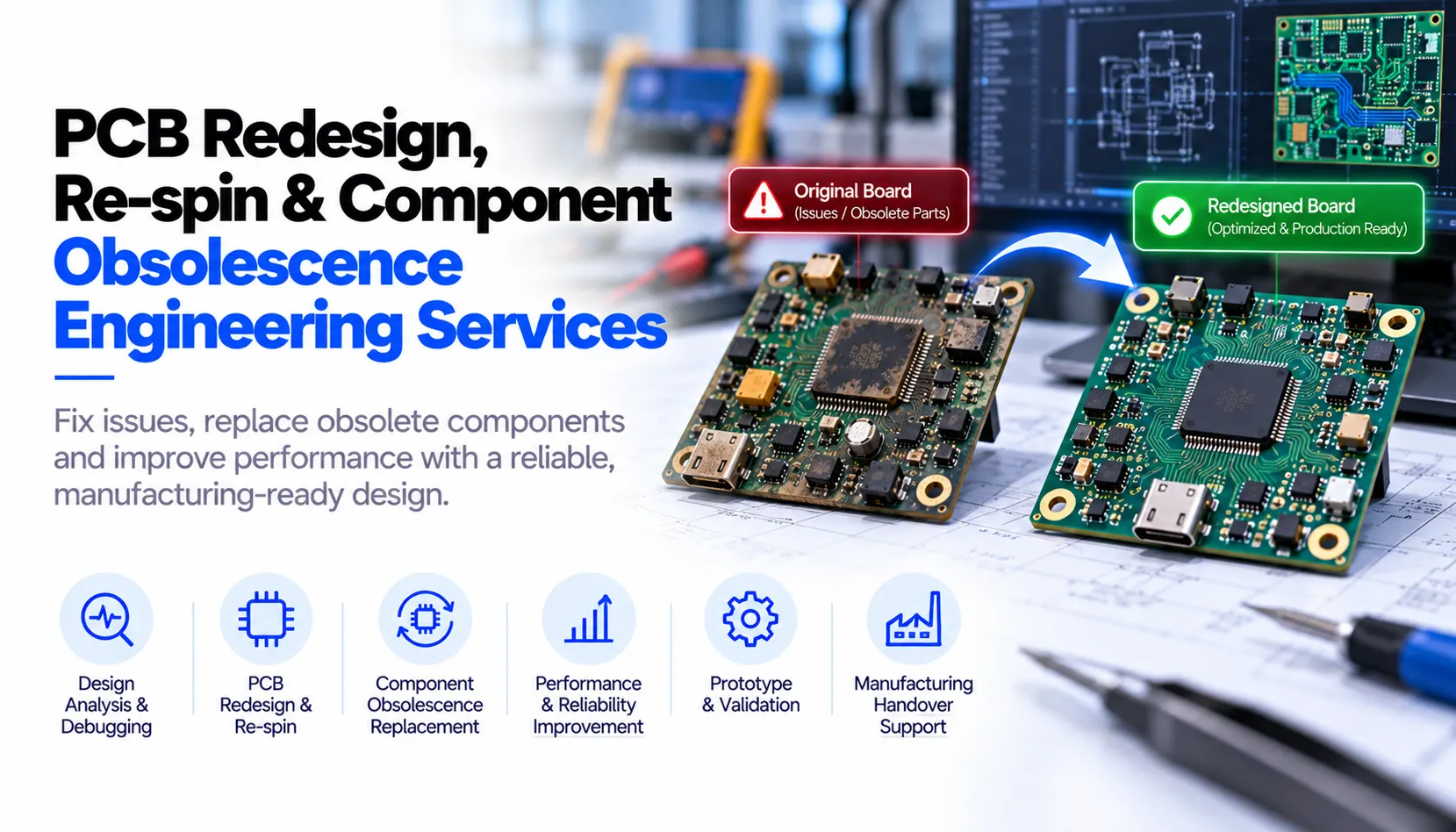
When is a PCB Design required to be Redone or Spun Again?
A spin design is one version of a PCB layout that is created with a purpose of changing or modifying the previous version. A spin is usually done after testing a prototype, determining compliance, checking for any faults in operation in the field or changing suppliers.
Some typical reasons for making a spin are:
The lack of stability while starting working of the CPU Faults at programming/debugging points Unstable operation of USB, Ethernet, memory or wireless interfaces Inefficient operation of power supply Noise picked by sensors caused by clocks, LEDs, motors Heating of the board inside the casing EMI/EMC testing shows high level of radiation Having problems with connectors, holes, and components dimensions according to casing design Making certain points hard to access during manufacturing A component being old or unavailable Reduced level of yield of the manufacturing process Reduction of price of manufacturing
A spin is done hurriedly without identifying the root cause of the problem.
How We Rescue an Existing PCB
Establish a Reliable Design Baseline
We begin by collecting the available schematic, PCB source, Gerber files, BOM, firmware, enclosure model, test records and known failure reports.
Not every inherited project has complete source files. When editable data is missing, we determine what can be recovered from fabrication outputs, assembled boards, photographs and measurements. Assumptions are recorded instead of silently being treated as facts.
We also identify the hardware revision used in each test. This prevents conclusions from one revision being applied incorrectly to another.
Reproduce the Failure
A problem that cannot be reproduced is difficult to fix confidently. We define the conditions under which the failure occurs: input voltage, temperature, load, cable, radio activity, firmware version and enclosure state.
Depending on the symptom, investigation may use an oscilloscope, logic analyser, power analyser, thermal camera, debugger or protocol tools. Inspection may also examine solder joints, footprints, polarity, assembly substitutions and manufacturing defects.
The purpose is to separate schematic faults, layout faults, component problems, firmware behaviour and assembly defects.
Control the Revision
Once the reason is known, we identify the smallest number of modifications appropriate for this situation. All changes are registered in a record of revisions and connected to a verification stage.
The new revision may consist of the schematic diagrams, native PCB files, output documents for fabrication, the BOM modifications, generally accepted alternatives, assembly drawings, upgrades of firmware, and testing instructions.
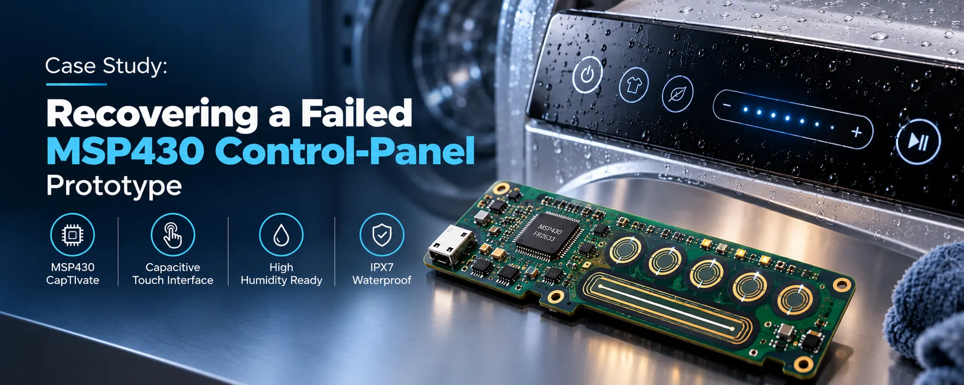
Case Study: Recovering a Failed MSP430 Control-Panel Prototype
The Client and the Initial Requirement
One of the medium-sized producers of household appliances later turned to Adequate Infosoft for the creation of a touch control panel capable of withstanding high humidity levels to be installed in a premium washing machine.
The developed product is based on a Texas Instruments MSP430FR2633 chip featuring CapTIvate technology. Among other things, it included five capacitive buttons, a sliding control bar, status LEDs, a USB-to-serial converter, and a glass covering.
The company was required to substitute the unreliable mechanistic controls with an interface possessing high resistance to wet cleaning and damp working environment.
The design used four PCB layers. Capacitive electrodes and sensitive routing occupied the top layer, a continuous ground reference was placed internally, and control, communication and LED connections were routed separately. Hatched copper beneath the sensing regions helped manage parasitic capacitance.
Failure Found During Board Bring-Up
The prototype that was first fully assembled passed the basic power and continuity tests but could not establish communications through the JTAG programming interface.
Instead of ordering another circuit board right away, the engineers went on to check the signals of the programming. The results obtained from an oscilloscope showed that the TCK clock line was constantly at 1.5 V instead of switching as expected at the logic level of 3.3 V.
The root cause was pin contention. The UART transmit and receive functions shared connections with the JTAG programming path, and the CP2102N USB-to-serial device was driving those lines while the programming probe was attached.
This was not a firmware defect or a defective microcontroller. It was an architectural conflict between two valid circuit functions.
The Re-spin
The board was revised to bring in zero-ohm resistor jumpers that can break the circuit between the serial transceiver and the processor.
This has provided the development and production teams with the means of achieving the isolation of the connections for programming purposes.
Layout design also solved another key issue observed during testing: it caused noise in the capacitive sensing paths from the LED switching.
The routes were separated into analog and digital, LED signals were routed from the opposite side of the board, and crossings were done at 90 degrees.
After the revision, the team completed programming and used TI's CapTIvate tools to tune the touch thresholds through a 2 mm glass surface.
Verification and Result
The new prototype underwent evaluation in environmental, EMI and thermal areas of study. The usage of PWM in LED control has cut down unnecessary digital activity. Furthermore, thermal pathways have enabled the device to function without a heatsink.
According to the published case study, the prototype took around 12 weeks to be completed, and features IPX7 waterproof rating and less mechanical wear parts.
The important outcome was not simply that a second PCB worked. The failure was measured, traced to a specific conflict, corrected through a controlled hardware revision and verified in the real product environment.
Component Obsolescence Engineering
A product can remain commercially useful long after one of its components reaches end of life. Obsolescence engineering keeps that product manufacturable without introducing uncontrolled design changes.
We review the BOM for:
End-of-life and not-recommended-for-new-design parts Manufacturer product-change notices Single-source dependencies Long or unstable lead times Unauthorised sourcing risks Parts with limited regional availability Components approaching lifecycle transitions
Just because a substitute is ideal does not mean that it comes from the closest datasheet match. A substitute must be assessed based on electrical characteristics, physical dimensions, layout, switching characteristics, start-up characteristics, thermal characteristics, firmware support, and compliance impacts.
Form, Fit and Function Analysis
Replacement may be physically compatible but not function in the same way. For example, regulators can behave differently in transient response, sensors may need new register maps, and memory components can differ in time characterizations.
Modules using a wireless connection can impact the overall safety certification. We note whether the selected part is suitable as a plug-and-play replacement, just needs a BOM update, needs modification of the firmware, or requires a change in layout.
Where appropriate, we can create alternate footprints, configurable component options or approved substitute lists to reduce future supply-chain risk.
Evidence from Related Delivered Projects
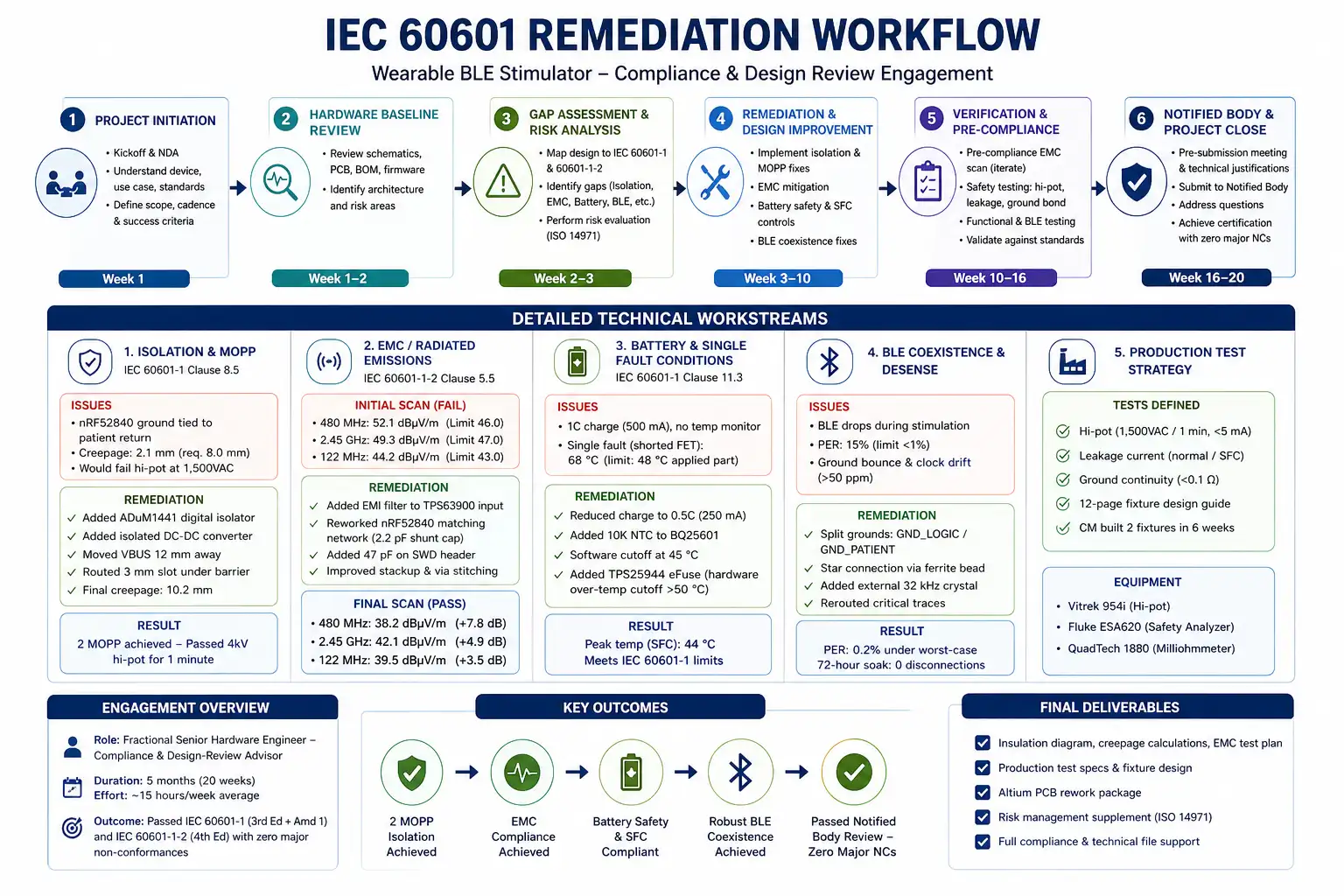
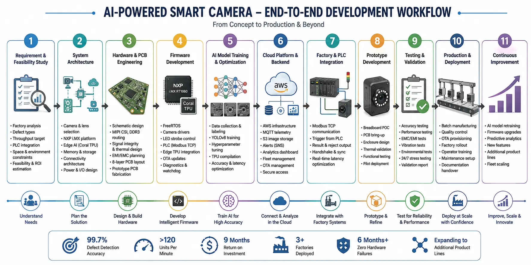
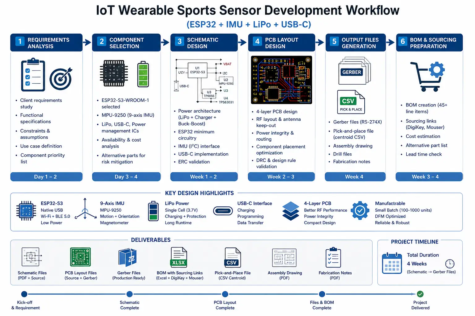
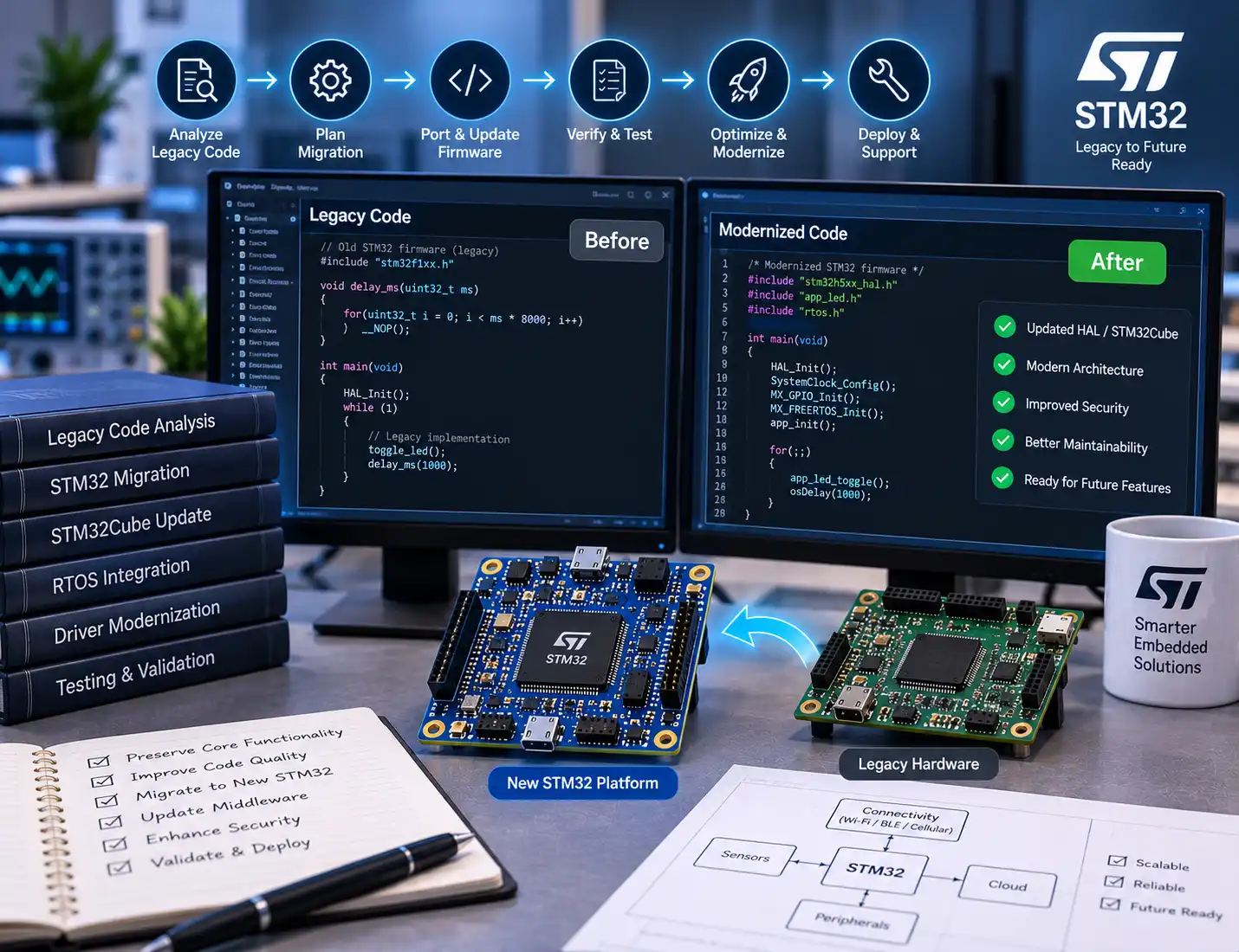
Recovering a circuit board is a process that necessitates a deep understanding of the physical prototypes involved, adherence to compliance regulations, and several iterations of design. Some lesser-known cases undertaken by Adequate Infosoft illustrate these aspects.
What We Check Before Releasing a New Revision
A revised board should answer the original failure and remain suitable for manufacturing. Our review can cover:
Schematic and PCB consistency Power-tree and sequencing behaviour Decoupling and return paths Clock, reset and boot configuration Programming and debugging access High-speed and differential routing RF antenna placement and matching provisions Thermal spreading and enclosure contact Component lifecycle and sourcing Footprints, polarity and assembly orientation DFM, DFT and test-point access Fabricator and assembly-house design rules
The verification plan is tied to the change list. If the re-spin modifies a power supply, we test startup, shutdown, peak load and fault behaviour. If it changes a communication interface, we exercise that interface under realistic traffic and environmental conditions.
Deliverables and Ownership of Design
The scope of the deliverables varies depending on the project. Some of the components include:
Finalized schematic and printed circuit board (PCB) files Documentation of all changes discussed and covered in the project Investigation report of the main cause of the problem established through the project Updated bill of materials and approved substitutions Output files for the creation of printed circuit boards Finished drilling, placing and assembly data A new version of a 3D board model Test protocol for the prototype created during the project Changes of the firmware and notes for the release Instructions for the production Requirements for testing the board in factory conditions
Ownership of the files, their licensing, and third-party dependencies are specified in the project agreement.
Bring Your Existing PCB Back to Production
It's not always the case that a failed prototype or an outdated component would require a complete redo of the process. It's often possible to keep some parts of the design and just work on the broken elements.
Share your PCB design and layout, schematic, parts list, firmware, tests, and assembled boards with Adequate Infosoft. We can evaluate your design and propose an optimal way to fix issues.
Frequently Asked Questions
Maybe. Gerber files will allow reconstructing the circuit board, but they do not have all required schematic information. We need to evaluate these files along with actual boards and documentation to evaluate the effort required for recovery.
Rework is valuable for confirming a suspected solution. A re-spin is normally appropriate when the correction must become repeatable, manufacturable and suitable for production.
Yes, but an MCU replacement may affect the footprint, peripherals, clocking, memory, firmware and programming process. We assess hardware and software migration together.
We attribute a particular reason and a test to every design change. All reviews, DFM checks, prototype launches, and revision logs help to avoid any surprises before the mass production stage.
Editorial Sources