


 Mean Stack Development
 Vue JS Development
 Javascript Development
 React JS Development
 Angular JS Development
 Next JS development
 Java Development
 Python Development
 Django Development
 Cherrypy Development
 C# Development
 ASP.NET Development
 NodeJS Development
 Laravel Development
 CodeIgniter Development
 Zend Development
 Ruby on Rails Development
 CakePHP Development
 PHP Website Development
 Symfony Development
 Drupal Development
 Joomla Development
 Wordpress Development
 .NET Nuke Development
 Kentico
 Umbraco
 .NET MAUI Development
 Xamarin Application Development
 iOS Application Development
 Android Application Development
 Android Wear App Development
 Ionic Development
 iBeacon Application Development
 Universal Windows Platform (UWP)
 Kotlin Application Development
 Swift Application Development
 Flutter Application Development
 PWA Application Development
 Flutter Health Tech & Wearable App Development Company
 React Native Health Tech Wearable App Development
 Offshore Software Development
 Custom Application Development
 Front-End Development
 Full Stack Development
 AI & Machine Learning
 Custom CRM Solutions
 Flask Software Development
 Electron JS Development
 ChatGPT Development
 Telemedicine App Development
 Build Smart Telemedicine Platform
 Beauty & Salon App Solutions
 Hire Workato Experts
 Magento Development
 Magento 2.0 Development
 Magento Enterprise
 Shopping Cart Development
 Prestashop Development
 Shopify Development
 Open Cart Development
 WooCommerce Development
 BigCommerce Development
 NopCommerce Development
 Virto Commerce Development
 AspDotNetStorefront Development
 .NET Application Development
 Microsoft Dynamics CRM
 VB .NET Development
 Sharepoint Migration
 ASP.NET Core Development
 ASP.NET MVC Development
 AJAX Development
 Agile Development
 Microsoft Bot
 Microsoft Blazor
 Microsoft Azure Cognitive
 HTML 5
 UI/UX Design
 Graphic Design
 Adobe Photoshop
 XML Application Development
 Cloud Computing Solutions
 Azure Cloud App Development
 AWS Development
 Google Cloud Development
 Certified AWS IoT Services Developers
 DevOps Consulting & Development
 Kubernetes Consulting & Services
 SQL Programming Development
 MySQL Development
 MongoDB Development
 Big Data
 Robotic Process Automation
 Social Media Marketing
 Search Engine Optimization
 QA Testing
 Software Testing
 Software Security
 Maintenance And Support
 I.T. Consulting Services
 Business Intelligence
 YII Development
 Data Analysis
 Alexa Skills Development
 On Demand App for Mobile repairing services
 On Demand App for Car Service Booking
 On Demand App for Cleaning Services
 On Demand App for Pharmacy
 On Demand Dedicated Developers
 On Demand Lawyer App Development












 Nuki Smart Lock
 Salto Smart Lock
 TTlock Smart Lock
 NFC App Development
 Custom IOT Enabled Smart Lock
 Smart Locker Solutions
 Hospital Smart Lock Systems
 Hotel Smart Lock Systems
 Smart Home & Office Locks
 Smart Access for Schools & Colleges
 Unloc Smart Lock Integration
 Yale & August Smart Lock Integration
 Populife Smart Lock Integration
 Smart Lock Hardware Development
 Dairy IoT Solutions
 Agri IoT & AI Solutions
 Weather & Climate Solutions
 Water & Waste Management Solutions
 RaspBerry Pi
 Firmware Software Development
 ESP 32 Software Development
 Embedded Development
 Internet of Things
 Smart IoT Development
 IoT Sensor Integration & Development Solutions
 Smart IoT System Development for HVAC
 Tuya IoT App Development
 Particle IoT SDK
 IoT Development with AI
 Smart Pet GPS Tracker
 Dairy GPS Tracking Solutions
 GPS Fleet Management Software
 Car Rental & Subscription Solutions
 Car Buy & Sell Marketplace Development
 AI-Powered Car Wash App Development
 PCB Design & Fabrication
 IoT AC Automation
 AI–IoT Painting Solutions
 IoT Wearable Hardware & App Development
 HVAC Automation & AI Control Systems
 Smart Home IoT Engineering
 AI Embedded Systems
 AI Hardware Design Service
 Advanced IoT Hardware & Firmware Development
 Device Driver Development Services
 NXP i.MX RT Firmware & Hardware Services
 Microchip PIC & AVR Development
 Hire IoT Architects
 IoT Cloud & Infrastructure Solutions
 Infineon XMC / AURIX Development Services
 Matter & Thread IoT Services
 Native IoT Mobile App Development (BLE & Wi-Fi)
 Snapdragon IoT Firmware Development
 Renesas RA/RX Firmware Services
 Silicon Labs EFR32 Development Services
 Smart Wearable App Development
 Smart IoT Meters
 Smart Healthcare Wearable App Development
 Health Care Monitoring System
 Fitness Tracking App Development
 Smart Home Automation Apps
 nRF PCB Design
 ESP32 PCB Design
 Embedded Wearables Engineers
 Rental Property Management System
 Building Management System
 Smart Lighting Development
 Infineon Semiconductor Firmware Development Services
 Custom Camera Development: Hardware, Firmware & PCB Prototyping
 Smart Security Camera SDK
 Nordic Semiconductor SDK
 Infineon SDK
 Arduino SDK
 NFC Lock Integration
 Kerong Lock Integration
 IoT & AI Solutions for Manufacturing
 Smart Inventory & Logistics Solution
 Food & Beverage Industry Solutions
 Smart Hospitality Solutions
 Smart Property Management
 Custom Smart Home IOT SDK
 Smart IoT & AI in Healthcare
 AI-Powered Security Solutions
 Smart Home Safety & AI
 Veterinary Clinic Management (AI)
 Pet Care System (AI & IoT)
 Pet Training & Adoption (AI)
 Healthcare IoT Development
 Event Management Software
 Money Remittance App
 Money Lending App Development
 Utility and Bill Payment App
 IoT Mobile App Development (Flutter & React Native)
 AI & IoT Retail Solutions
 Smart EV App Development
 Smart Solar IoT & AI Solutions
 IoT-Based Energy Systems
 Smart Energy & Utilities Solutions
 6G Solutions
 IoT Security Solutions
 AI-Powered Lottery App Development
 AI-Sports Fitness Club Management
 Travel
 Real Estate
 Medical & Healthcare
 e-Learning
 Consumer Products
 Finance
 Automobile
 Media & Entertainment
 Billing Software
 Enterprise Resource Planning (ERP)
 Augumented & Virtual Reality
 Point of Sale(POS) Development
 Learning Management System
 EV Charging Solutions
 About Us
 Partners & Certifications
 Quality Assurance
 Our Clients & Testimonials
 Development Process
 Our Products
 Social Responsibility
 Work Ethics
 Vision & Mission
 Awards
 Live Project Demos
 Contact Us
 Case Studies
 Portfolio
 Blog
Mixed-Signal & Analog PCB Design Services | Low-Noise Hardware Experts
Mixed-signal devices involve the integration of two opposite electrical situations in one PCB. Delicate analog signals may exist within microvolt or millivolt range, whilst processors, radio broadcast and receiver equipment, clock circuits and switching power supplies create high-frequency pulses and broadband noise just a few millimeters away.
A circuit board can have a correct schematic diagram but fail due to improper arrangements, uncontrolled return currents, insufficient decoupling or connection between analog and digital parts.
Adequate Infosoft provides mixed-signal PCB design and analog PCB design services for IoT devices, medical wearables, industrial sensors, audio products, smart-energy systems and battery-powered electronics.
We support the complete engineering cycle, including requirements analysis, component selection, schematic development, circuit simulation, multilayer PCB layout, prototyping, board bring-up and design optimization.
Our objective is not simply to produce manufacturing files. We develop a board that can measure, process and communicate real-world signals reliably within the product's mechanical, power, cost and regulatory constraints.
Let's Work Together!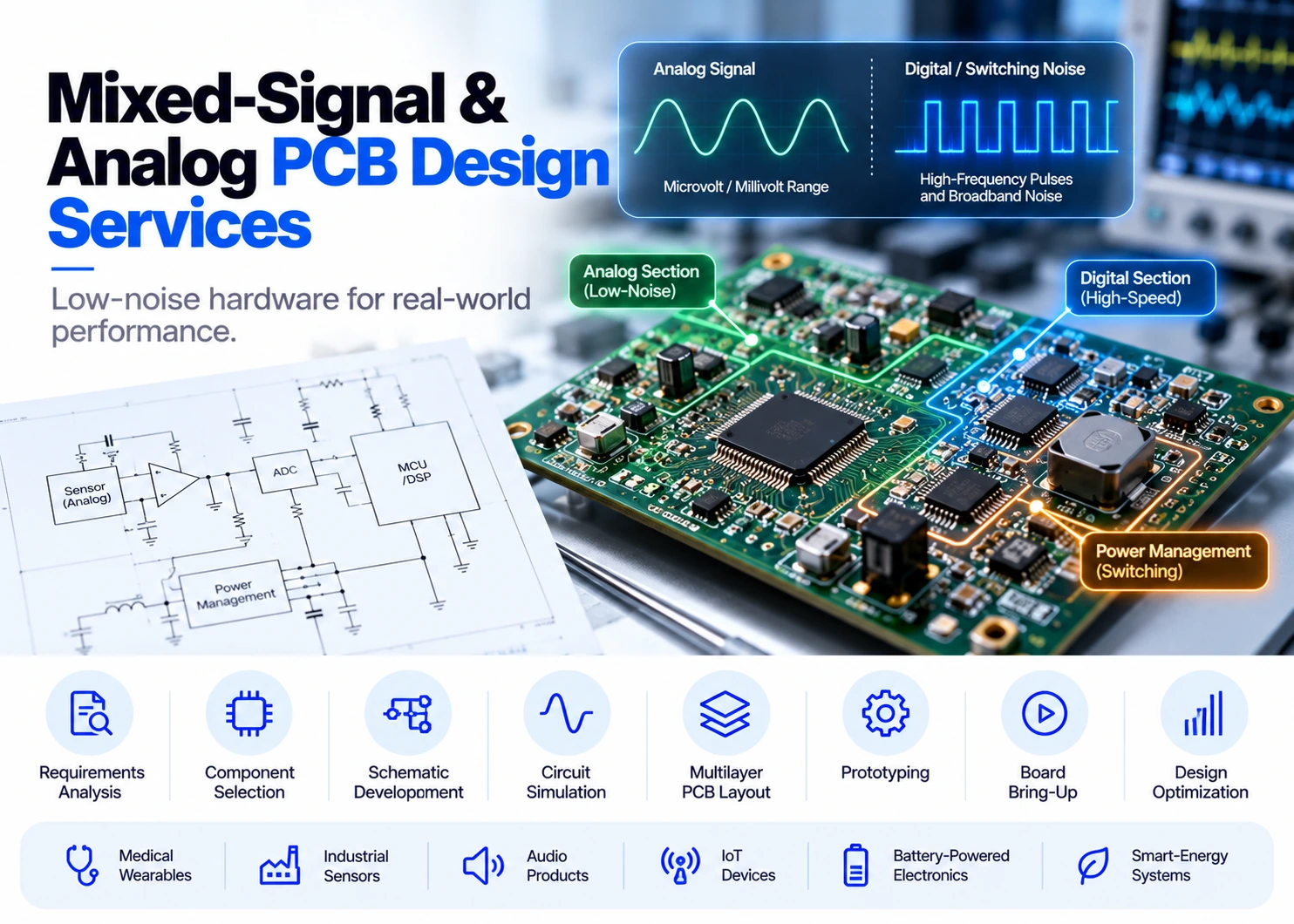
What Is a Mixed-Signal PCB?
A mixed-signal PCB contains analog and digital circuits within the same system. Common examples include:
A sensor signal processed by an analog front end and ADC A microphone input connected to an audio codec and microcontroller A DAC driving an analog actuator or amplifier A medical wearable combining biopotential measurement with Bluetooth An industrial controller with voltage, current or temperature inputs A smart meter with measurement circuits, an MCU and wireless connectivity
As digital circuits usually tolerate small interferences due to the specific logic levels, precision analog circuit accepting analog signals tend to be less tolerant of noise. Indeed, noise that is getting into amplifier, reference voltage or ADC input may diminish the usable resolution, cause false readings or introduce some distortion.
This is why effective mixed-signal design relies not just on separation of the board into well-defined digital and analog sections, but on the understanding of where the current flows in a circuit.
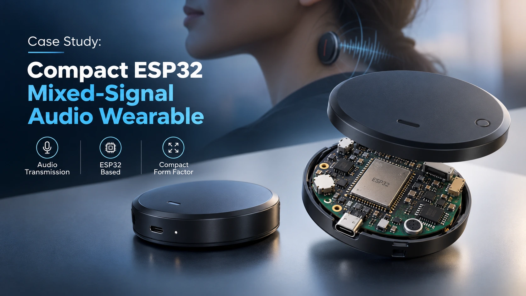
Case Study: Compact ESP32 Mixed-Signal Audio Wearable
Client and Product Requirement
An international client from the wearable technology sector reached out to Adequate Infosoft in order to create the schematic and PCB of a prototype that uses the ESP32 module for the purpose of audio transmission.
The details regarding the identity of the client are not revealed due to the mutual NDA, however, the product and engineering work done by Adequate Infosoft is covered in the published portfolio.
The device was supposed to be built into a cylindrical casing with a diameter of around 46 mm and the height of about 10.5 mm.
Within that confined space, the board had to integrate an ESP32 microcontroller, power management electronics, sensors, and a complete solution that enables audio processing.
The challenge was more complex than fitting components into the enclosure. The analog audio stages had to operate beside the ESP32's clocked digital logic and wireless functions. Poor placement or routing could introduce audible interference, reduce signal quality or make prototype testing unreliable.
Engineering Approach
We started with a thorough review of product architecture and audio chain requirements, as well as the available throughput and the related mechanical constraints. We made sure that all the mixed-signal sections were determined before placing the components to avoid having signals sensitive to noise passing through digital components in the layout stage.
The ADC, DAC, and related analog components were positioned such that we kept input and output circuits short. We routed digital communication lines in such a way as to avoid parallel coupling with analog traces, while ensuring that high-speed paths contained controlled return paths and decoupling capacitors that had been positioned in close vicinity to the devices they served.
The power system was reviewed as part of the signal-integrity strategy. Switching-current loops were kept compact, and sensitive analog circuitry was positioned away from noisy power nodes. Grounding and signal-return behaviour were considered together rather than relying on an arbitrary board split.
Because enclosure height and diameter were fixed, placement also had to accommodate connectors, test access and practical assembly. Mechanical limitations were reviewed alongside the electrical design so the finished layout could be manufactured and installed in the intended enclosure.
We included accessible test points for important rails and signals. These enabled the client's engineers to perform structured prototype bring-up, inspect the audio chain and identify whether unexpected behaviour originated in the analog circuitry, firmware or power system.
Deliverables and Result
Adequate Infosoft provided the client with the needed documentation of the finalized schematic, mixed-signal PCB design, components selection process and PCB layout, which was necessary for prototyping. The done design assignment afforded the client an effective means of small-scale assembly, bench tests, and product improvement.
Most importantly, the project translated a constrained product concept into a prototype-ready hardware design while addressing the interaction among analog audio, high-speed digital processing, power management and mechanical packaging.
This engagement demonstrates our ability to treat mixed-signal PCB development as a system-level engineering task. We considered the enclosure, signal chain, return paths, power architecture, testing requirements and manufacturability together instead of optimizing each area in isolation.
Relevant Projects That Demonstrate Our Experience
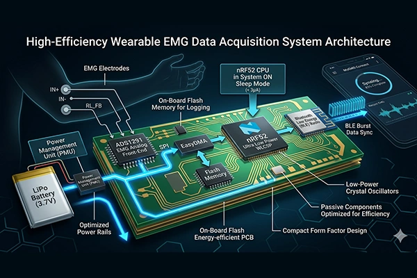
Our mixed-signal capabilities are supported by practical projects published on the Adequate Infosoft website.
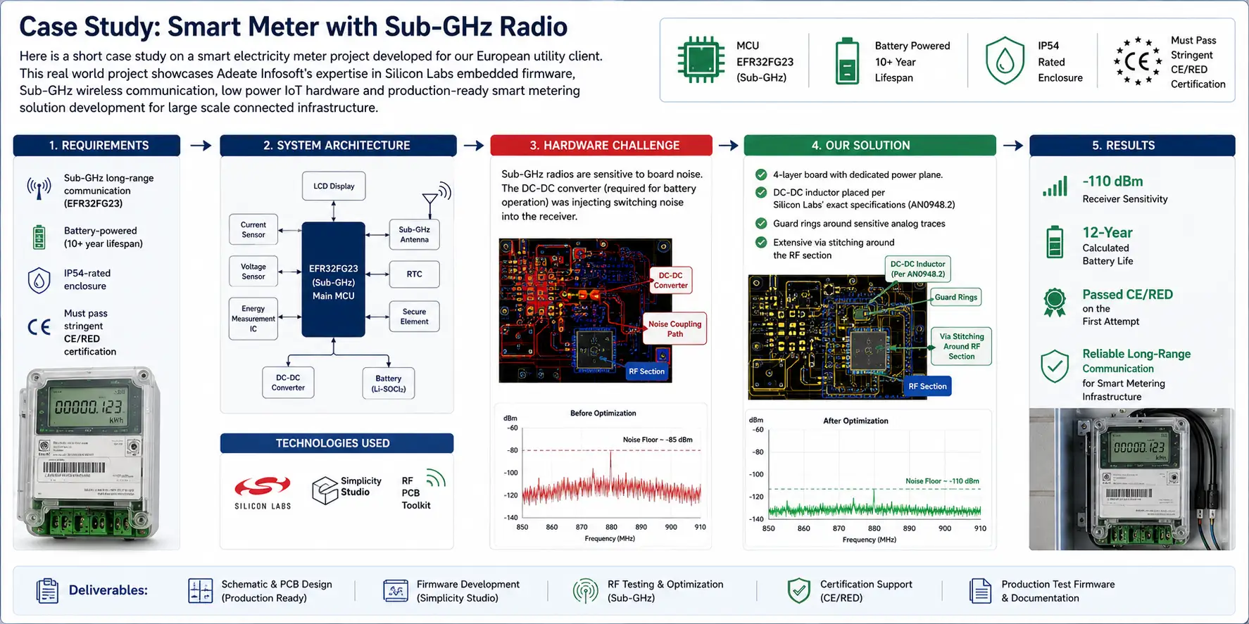
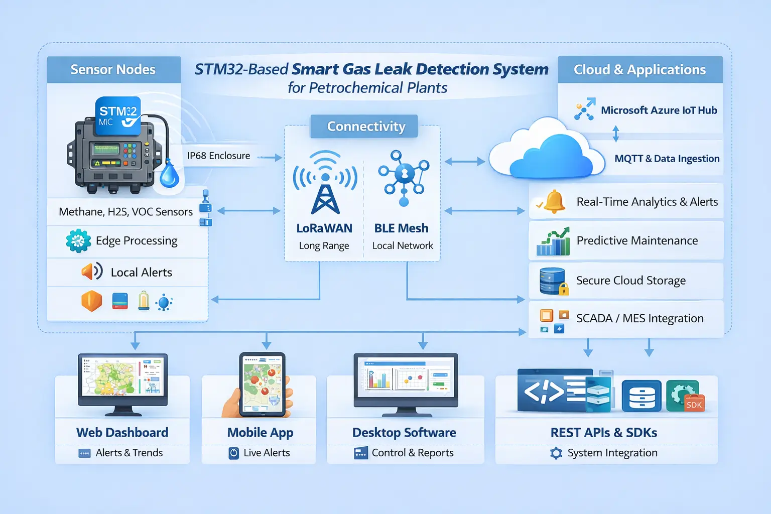
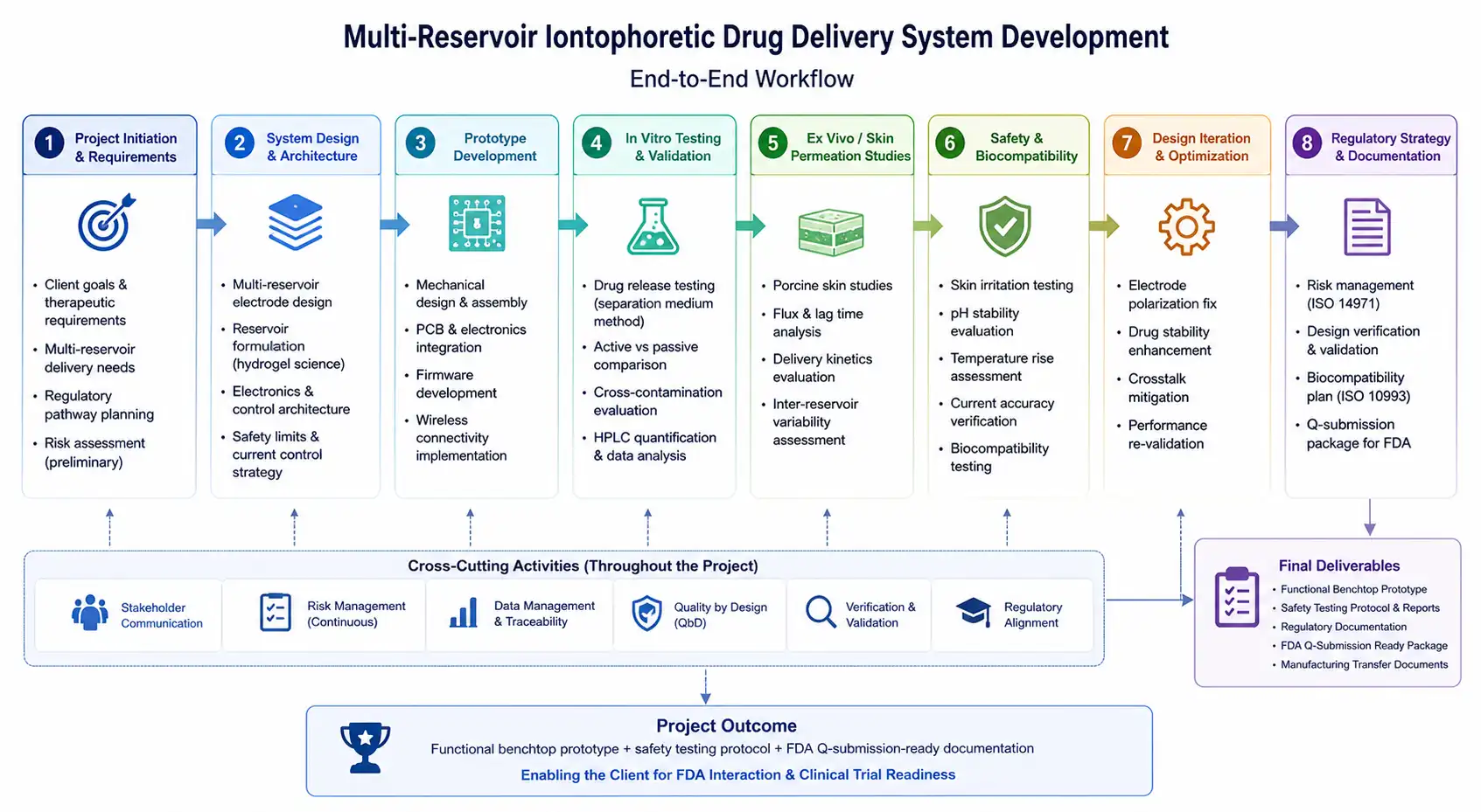
Our Mixed-Signal and Analog PCB Design Services
Design of Analog Circuits and Schematics
The circuits we produce are used for sensor conditioning, amplification, filtering, conversion and protection. The configurations of the circuits vary according to the requirements of the specific project, and may involve using operational amplifiers, instrumentation amplifiers, ADCs, DACs and audio codecs, comparators, current sensors and precision voltage devices.
For each circuit we assess its elements against functional requirements including input range, bandwidth, noise density, offset, drift, common-mode range, power consumption and availability.
Design of Analog Front-End
Analog front-end plays a key role in terms of the quality of information which is passed on to the processor. Our engineers are working on the design of the front ends for temperature, pressure, current and voltage, vibration, audio, gas, optical and biopotential sensors.
The work may include such processes as matching impedance, anti-alias filtering, gain adjustment, protection and biasing of input, and using differential signals. We always analyze the whole signal path so that amplifier noise, ADC accuracy and reference value correlate to the data instead of being considered separately.
ADC and DAC Integration
High-resolution data converters require careful power, reference, grounding and layout decisions. We help select and integrate suitable SAR, delta-sigma and audio converters based on sample rate, resolution, latency and power requirements.
Converter selection is only the beginning. Reference bypassing, driver settling, input filtering, clock quality and return-current control can directly affect effective performance. We place supporting components close to the relevant pins and keep sensitive converter inputs away from clocks, switching nodes and wireless sections.
Low-Noise PCB Layout
Our mixed-signal layout process begins with functional partitioning. Sensitive analog components are grouped around the signal source, while processors, memory, displays and communication devices are positioned according to their digital and high-speed requirements.
We maintain short analog paths, uninterrupted return paths and controlled placement of domain boundaries. Clocks and fast digital traces are prevented from crossing sensitive analog regions. Power regulators are positioned so their switching-current loops remain compact and separated from measurement circuitry.
Grounding is derived from the converter system, its design and the paths of currents. We do not follow a single rule of split grounding. In some systems, the use of ground pads has been ineffective while applying a continuous ground plane with proper placement and routing is a better solution than a simple split ground.
Analog Devices and Texas Instruments stress the importance of placement, routing and control of return current paths in mixed-signal board designs.
Power-Supply and Reference Design
In order to create a low noise signal chain, it is crucial to have clean and stable power supply. We design our regulator stages by using appropriate LDOs, DC-DC converters, ferrite beads, bulk capacitors and local decoupling. In cases where switching conversion is required, we evaluate switching frequency, harmonic content, load transients and distance to sensitive electronics.
Separate supply filtering may be used for ADCs, references, amplifiers and radio sections. Component placement and current-loop area are treated as part of the power design—not as tasks left until routing.
Simulation, Prototyping and Testing
We apply signal and circuit analysis depending on the task at hand in order to perform evaluations such as gain, bandwidth, stability, filtering, and component tolerances before actual manufacturing.
When the board has been assembled, it can be tested using techniques such as rail sequencing, measurement of power consumption, analysis of the signal chain, measurement of the noise floor, communication testing, and thermal testing.
We can also provide design files, Gerbers, drill data, assembly drawings, pick-and-place files, bill of materials and engineering notes for prototype or production transfer.
Why Choose Adequate Infosoft?
Mixed signal development is hardly a project that requires only layout work. A competent engineering partner should be knowledgeable in sensors, analog electronics, embedded processors, power supply, wireless communication, firmware, and product parameters.
Adequate Infosoft offers:
Schematic, PCB, firmware, and IoT knowledge combined in a single engineering team Experience in ESP32, STM32, Nordic, NXP, Silicon Labs and TI platforms Expert knowledge of ADC, DAC, sensor interfaces, and the analog front end Capabilities in rigid multilayer and compact wearables PCB designs Prototype bringing, debugging and design review services Documentation and components ready for production Product development in accordance with NDA
You can count on us whether you need to create a new product from scratch or solve issues with an existing board, such as noise, accuracy, or stability.
Discuss Your Mixed-Signal PCB Project
If your product includes sensors, audio, precise measuring, wireless transmission and processing with embedded technology, the layout decisions made in the early stages may influence whether the first prototype operates as planned.
Provide Adequate Infosoft with your requirements, block diagram, housing limitations or previous design. Our specialists will help you create a stable, testable and applicable mixed-signal PCB from the very initial connection scheme to validation.
Frequently Asked Questions
Definitely. The schematic of the board will be examined along with its stack-up, placement of components and regulating circuits, routing of signal and return currents. After that, complete PCB re-layout or selective design corrections can be performed.
Yes. Our embedded team can develop ADC acquisition, sensor drivers, calibration, filtering, digital signal processing, BLE, Wi-Fi and other device firmware alongside the hardware.
Yes. Our portfolio includes wearable sensing, EMG acquisition, haptic feedback and battery-powered designs. Regulatory certification depends on the final product and test laboratory, but we can design with the relevant safety, testability and documentation requirements in mind.
Standard deliverables often consist of source schematics, PCB layout files, Gerber files, drill files, fabrication drawings, assembly drawings, pick-and-place information, BOM and design notes. Confirmations for the contents of deliverables are received before the project starts.
Editorial Sources