


 Mean Stack Development
 Vue JS Development
 Javascript Development
 React JS Development
 Angular JS Development
 Next JS development
 Java Development
 Python Development
 Django Development
 Cherrypy Development
 C# Development
 ASP.NET Development
 NodeJS Development
 Laravel Development
 CodeIgniter Development
 Zend Development
 Ruby on Rails Development
 CakePHP Development
 PHP Website Development
 Symfony Development
 Drupal Development
 Joomla Development
 Wordpress Development
 .NET Nuke Development
 Kentico
 Umbraco
 .NET MAUI Development
 Xamarin Application Development
 iOS Application Development
 Android Application Development
 Android Wear App Development
 Ionic Development
 iBeacon Application Development
 Universal Windows Platform (UWP)
 Kotlin Application Development
 Swift Application Development
 Flutter Application Development
 PWA Application Development
 Flutter Health Tech & Wearable App Development Company
 React Native Health Tech Wearable App Development
 Offshore Software Development
 Custom Application Development
 Front-End Development
 Full Stack Development
 AI & Machine Learning
 Custom CRM Solutions
 Flask Software Development
 Electron JS Development
 ChatGPT Development
 Telemedicine App Development
 Build Smart Telemedicine Platform
 Beauty & Salon App Solutions
 Hire Workato Experts
 Magento Development
 Magento 2.0 Development
 Magento Enterprise
 Shopping Cart Development
 Prestashop Development
 Shopify Development
 Open Cart Development
 WooCommerce Development
 BigCommerce Development
 NopCommerce Development
 Virto Commerce Development
 AspDotNetStorefront Development
 .NET Application Development
 Microsoft Dynamics CRM
 VB .NET Development
 Sharepoint Migration
 ASP.NET Core Development
 ASP.NET MVC Development
 AJAX Development
 Agile Development
 Microsoft Bot
 Microsoft Blazor
 Microsoft Azure Cognitive
 HTML 5
 UI/UX Design
 Graphic Design
 Adobe Photoshop
 XML Application Development
 Cloud Computing Solutions
 Azure Cloud App Development
 AWS Development
 Google Cloud Development
 Certified AWS IoT Services Developers
 DevOps Consulting & Development
 Kubernetes Consulting & Services
 SQL Programming Development
 MySQL Development
 MongoDB Development
 Big Data
 Robotic Process Automation
 Social Media Marketing
 Search Engine Optimization
 QA Testing
 Software Testing
 Software Security
 Maintenance And Support
 I.T. Consulting Services
 Business Intelligence
 YII Development
 Data Analysis
 Alexa Skills Development
 On Demand App for Mobile repairing services
 On Demand App for Car Service Booking
 On Demand App for Cleaning Services
 On Demand App for Pharmacy
 On Demand Dedicated Developers
 On Demand Lawyer App Development











 Nuki Smart Lock
 Salto Smart Lock
 TTlock Smart Lock
 NFC App Development
 Custom IOT Enabled Smart Lock
 Smart Locker Solutions
 Hospital Smart Lock Systems
 Hotel Smart Lock Systems
 Smart Home & Office Locks
 Smart Access for Schools & Colleges
 Unloc Smart Lock Integration
 Yale & August Smart Lock Integration
 Populife Smart Lock Integration
 Smart Lock Hardware Development
 Dairy IoT Solutions
 Agri IoT & AI Solutions
 Weather & Climate Solutions
 Water & Waste Management Solutions
 RaspBerry Pi
 Firmware Software Development
 ESP 32 Software Development
 Embedded Development
 Internet of Things
 Smart IoT Development
 IoT Sensor Integration & Development Solutions
 Smart IoT System Development for HVAC
 Tuya IoT App Development
 Particle IoT SDK
 IoT Development with AI
 Smart Pet GPS Tracker
 Dairy GPS Tracking Solutions
 GPS Fleet Management Software
 Car Rental & Subscription Solutions
 Car Buy & Sell Marketplace Development
 AI-Powered Car Wash App Development
 PCB Design & Fabrication
 IoT AC Automation
 AI–IoT Painting Solutions
 IoT Wearable Hardware & App Development
 HVAC Automation & AI Control Systems
 Smart Home IoT Engineering
 AI Embedded Systems
 AI Hardware Design Service
 Advanced IoT Hardware & Firmware Development
 Device Driver Development Services
 NXP i.MX RT Firmware & Hardware Services
 Microchip PIC & AVR Development
 Hire IoT Architects
 IoT Cloud & Infrastructure Solutions
 Infineon XMC / AURIX Development Services
 Matter & Thread IoT Services
 Native IoT Mobile App Development (BLE & Wi-Fi)
 Snapdragon IoT Firmware Development
 Renesas RA/RX Firmware Services
 Silicon Labs EFR32 Development Services
 Smart Wearable App Development
 Smart IoT Meters
 Smart Healthcare Wearable App Development
 Health Care Monitoring System
 Fitness Tracking App Development
 Smart Home Automation Apps
 nRF PCB Design
 ESP32 PCB Design
 Embedded Wearables Engineers
 Rental Property Management System
 Building Management System
 Smart Lighting Development
 Infineon Semiconductor Firmware Development Services
 Custom Camera Development: Hardware, Firmware & PCB Prototyping
 Smart Security Camera SDK
 Nordic Semiconductor SDK
 Infineon SDK
 Arduino SDK
 NFC Lock Integration
 Kerong Lock Integration
 IoT & AI Solutions for Manufacturing
 Smart Inventory & Logistics Solution
 Food & Beverage Industry Solutions
 Smart Hospitality Solutions
 Smart Property Management
 Custom Smart Home IOT SDK
 Smart IoT & AI in Healthcare
 AI-Powered Security Solutions
 Smart Home Safety & AI
 Veterinary Clinic Management (AI)
 Pet Care System (AI & IoT)
 Pet Training & Adoption (AI)
 Healthcare IoT Development
 Event Management Software
 Money Remittance App
 Money Lending App Development
 Utility and Bill Payment App
 IoT Mobile App Development (Flutter & React Native)
 AI & IoT Retail Solutions
 Smart EV App Development
 Smart Solar IoT & AI Solutions
 IoT-Based Energy Systems
 Smart Energy & Utilities Solutions
 6G Solutions
 IoT Security Solutions
 AI-Powered Lottery App Development
 AI-Sports Fitness Club Management
 Travel
 Real Estate
 Medical & Healthcare
 e-Learning
 Consumer Products
 Finance
 Automobile
 Media & Entertainment
 Billing Software
 Enterprise Resource Planning (ERP)
 Augumented & Virtual Reality
 Point of Sale(POS) Development
 Learning Management System
 EV Charging Solutions
 About Us
 Partners & Certifications
 Quality Assurance
 Our Clients & Testimonials
 Development Process
 Our Products
 Social Responsibility
 Work Ethics
 Vision & Mission
 Awards
 Live Project Demos
 Contact Us
 Case Studies
 Portfolio
 Blog
High-Speed PCB Design & Signal Integrity Services
A board that has powered on successfully might face problems when it comes to its interfaces functioning properly. USB connections may fail during transfer.
The camera images may be corrupted. Memory problems only show up after the device warms up, Ethernet may work with one cable and not work with a different cable.
These issues occur due to the issues with the sending and receiving paths, proper power delivery, connectors, component selection, and proper firmware configuration. Fixing these problems is possible only after analyzing the whole electrical path.
Adequate Infosoft provides high-speed PCB design and signal integrity services for embedded products, camera systems, robotics, industrial electronics, and connected devices. Our published projects include custom carrier boards, multilayer hardware, and interface integration supported by embedded software development.
The objective is straightforward: create hardware that transfers data reliably, can be tested effectively, and is documented for manufacturing and future revisions.
Let's Work Together!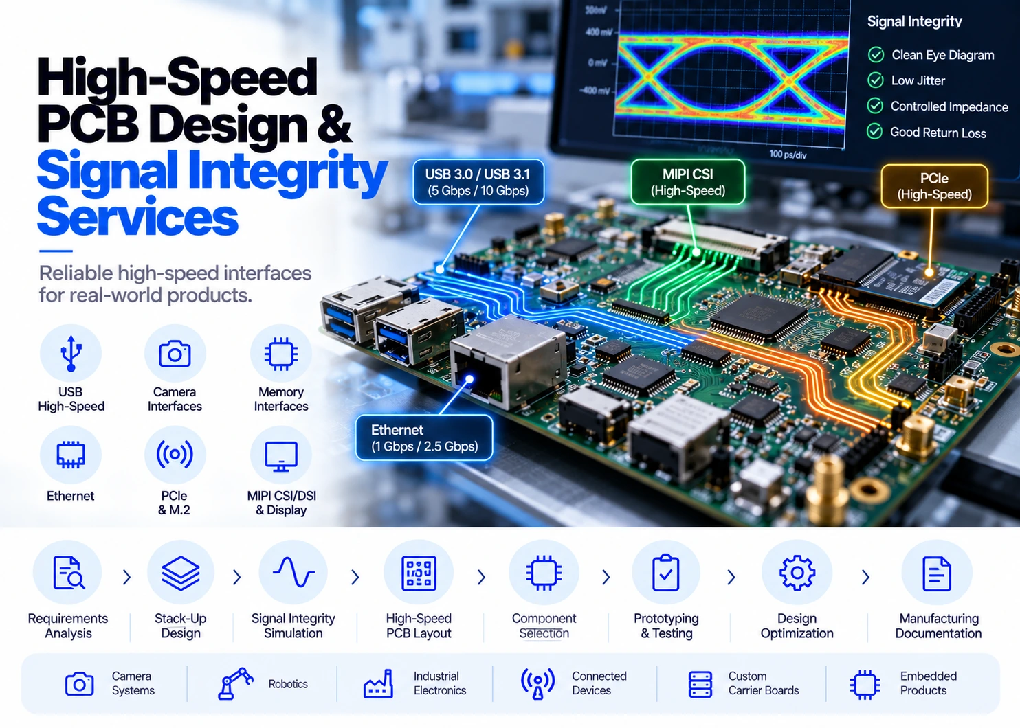
What Is High-Speed PCB Design?
High-speed PCB design focuses on the action of fast signals as they pass though PCB traces, via holes, connectors, and wires.
It is not just the clock frequency that determines if the connection should be treated appropriately for high speed. The rise time and fall time of the signal, track length and propagation delay have to be taken into consideration properly together with any other factors determining if the effects of transmission line become important.
Signal integrity is if the receiver detects the correct waveform at the right time. Reflections, crosstalk, losses, and errors regarding timing lower that margins. Power integrity is if the component gets stable power in changing conditions.
Case Study: Jetson Orin Nano Carrier Board for a Warehouse Robotics Client
Client Background and Project Requirement
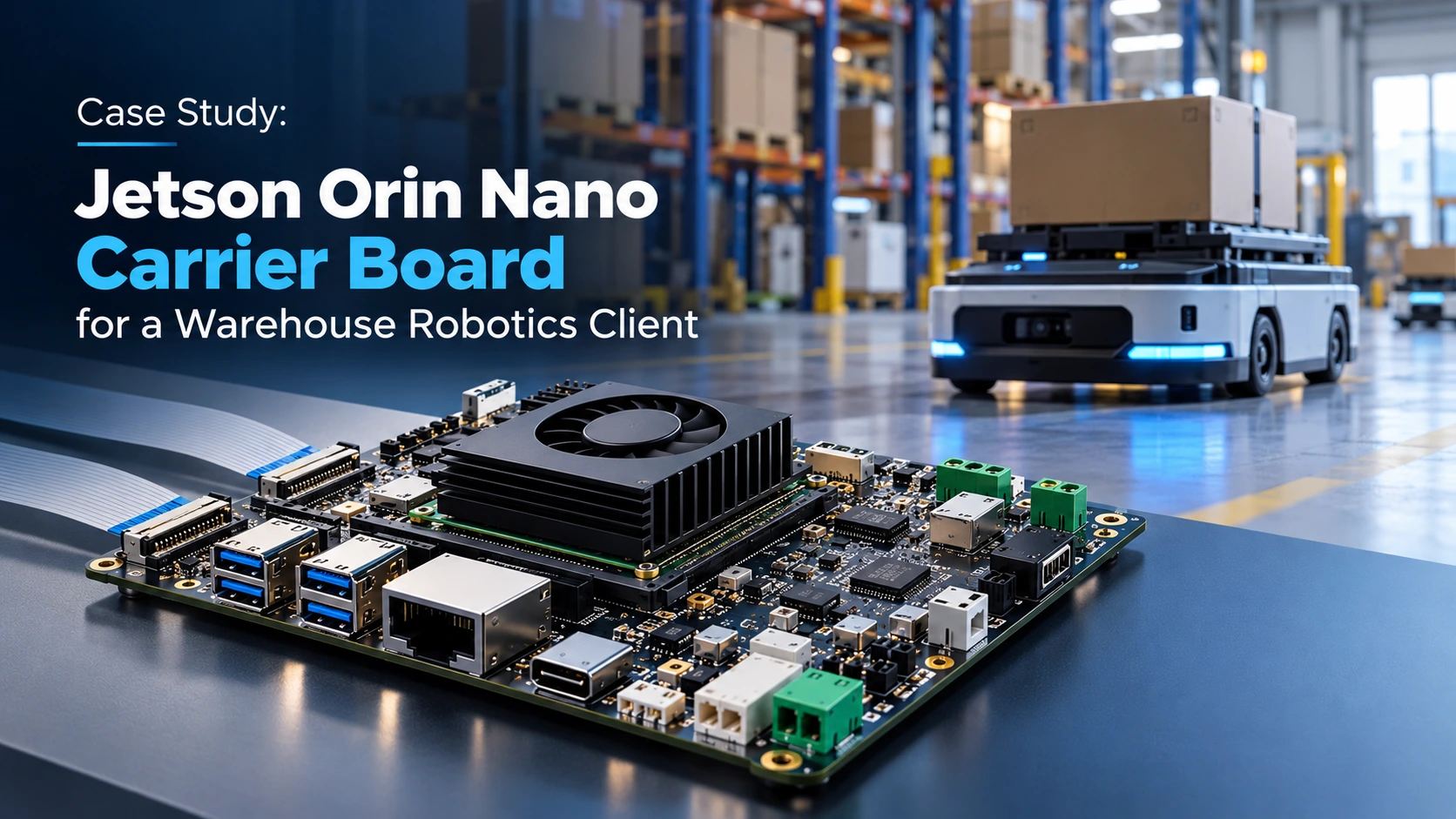
We published a robotics case study about a logistics and transport firm that wants to automate the internal material transport within the warehouse. The company's name has not been released.
The solution involved a combination of the NVIDIA Jetson Orin Nano computing platform, an STM32-based motor controller, and ROS 2 software.
For the electronics, the challenge was integration: computing, sensing, communication, and motor control had to operate within one mobile system. The carrier board therefore formed an important connection between the processing module and the robot's external devices.
Documented PCB Architecture
The published paper explains a custom six-layer carrier board type Jetson with camera connections, USB 3.0, Gigabit Ethernet, UART, CAN, and M.2 wire structure.
It elaborated on dedicated power distribution, filtering components, thermal properties, and grounding measures. A separate dedicated custom controller was responsible for motor actuation.
This architecture demonstrates relevant experience integrating fast digital interfaces with power electronics and embedded control. The following engineering discussion explains the significance of that arrangement; it does not introduce additional unpublished measurements or test results.
Why the High-Speed Interfaces Need Separate Rules
Different functions and electrical requirements are served by the Camera, USB and Ethernet connections. The routing restrictions of each of them should be determined from the module, interface and component literature.
For example, the camera connection must provide the correct lane configuration, allowed skew and interconnection assumptions. In the case of USB routing, the entire path through the board and connector has to be determined. As for Ethernet, this depends on the implementation of the physical layer chosen.
NVIDIA's carrier-board guidance provides interface-specific requirements, illustrating why a single generic differential-pair rule is insufficient for this class of product.
Engineering Lessons for Power and Return Paths
A robot introduces changing loads as motors accelerate, sensors operate, and processing demand increases. These operating states make power distribution and grounding important parts of interface reliability.
For a comparable design, review should examine whether fast signals retain suitable reference planes and whether switching-current paths disturb sensitive circuits. Placement decisions can reduce the need for difficult routing corrections later.
The lesson is to plan signal and power paths together. Treating the carrier board as a collection of connectors can overlook the electrical interactions that emerge during operation.
Validation Priorities and Buyer Value
A good validation plan for this architecture would incorporate testing of camera transmission, USB activity, network flow, and varying load. It should also define acceptable behavior, thereby allowing one to distinguish electrical faults from either driver issues or ones related to the software configuration.
The availability of programming interfaces, diagnostic prints, and hardware updates could make the detection of faults easier.
This project's relevance lies in the documented integration of a custom carrier board into a complete robotic platform. It supports our experience in embedded hardware integration. Exact channel margins, compliance results, and production yield must still be demonstrated through the records and acceptance tests agreed for each new engagement.
Relevant Delivered Projects That Support Our Experience
Our published portfolio provides further evidence of PCB development and interface integration. Each example below identifies its specific relevance rather than treating every embedded project as proof of every high-speed capability.
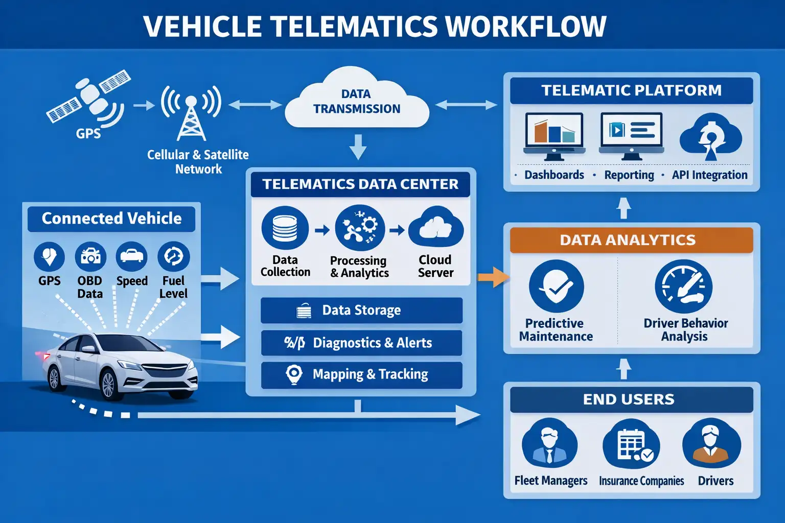
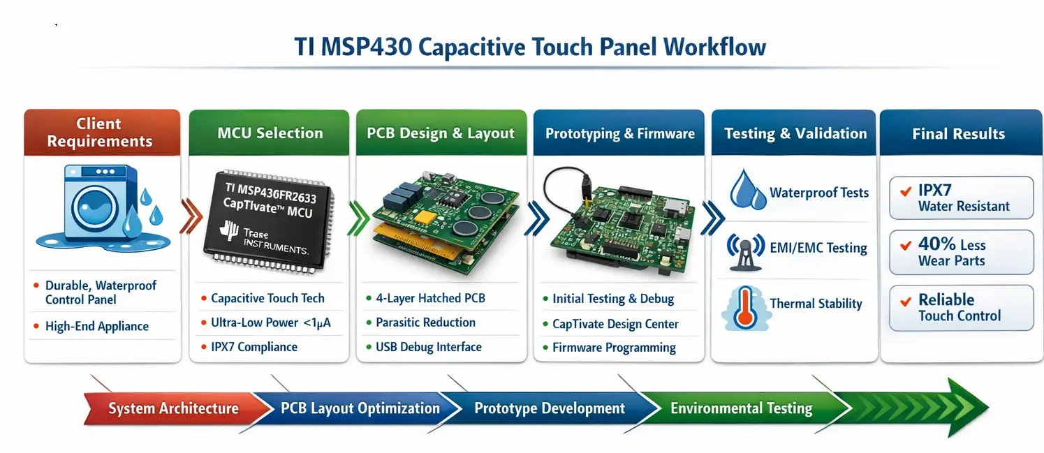
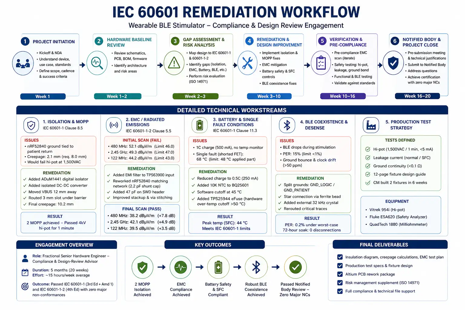
Our High-Speed PCB Design Services
PCB Stack-Up and Controlled-Impedance Planning
The process of stack-up planning starts before the routing procedures are worked out. It is the layer assignment, dielectric thickness of layers, types of copper used, and properties of the materials used that dictates the value of impendence and losses of the most important connections.
We create the routing needs based on the selected components and the fabricator's specifications. Engineering drawings need to provide the required impedances and permitted tolerances rather than letting the vendors deal with them.
More layers make routing easier, but the right stack-up depends on the technology integrated, continuity of reference planes, dimensions and costs.
Differential-Pair Routing and Return Paths
There are a number of factors to consider in USB, PCIe, Ethernet, and camera designs. Not being able to apply a single impedance and length-matching rule creates a design dilemma.
Other factors such as routing, symmetry of pairs, skew, transitions with connectors, via location, and location of signals should also be considered.
Unnecessary layer switching and routing through holes can lead to discontinuities in the design. It is important to plan for a return path whenever there is a signal transition.
DDR Memory and Timing-Aware Layout
The routing of DDR is based on the specifications given by the memory controller for topology, termination, impedance, and timing.
In doing so, the data signals are routed with their strobe signals, while routing for address, clock, and command signals is performed according to the instructions provided by the controller. One must understand that keeping all traces of the same length does not mean that one is taking into consideration the timing groups.
Also, package delays, layer propagation, and capabilities of the controller have an influence on the routing budget. The requirements should be referred to the documentation provided by the processor and memory chosen.
Signal Integrity Analysis and Power Delivery Review
The project requirements may affect the type of analysis used, such as studying reflections, terminations, coupling, channel attenuation, or timing margins.
The simulation conditions matter, which require recording the driver models, interconnects and properties of stack-up and operating conditions.
Power delivery review considers regulator behavior, decoupling placement, current paths, sequencing, and voltage variation under load. A clean-looking signal route cannot compensate for an unstable supply.
Manufacturing, Testing, and Design Ownership
It is crucial for the professional PCB buyers to be involved in the handover and in the fabrication process which should be essentially standardized.
The choice of components should depend on the expected life cycle of the component, lead time, and sourcing technique that are already approved. Changing a connector, protection component, or memory part might change the electrical characteristics of the circuit, which implies the reference design revision.
Design for manufacture means creating a PCB design according to the limitations of the fabrication and assembly process. Design for test makes the design suitable for debugging activities by ensuring easy access to programming, measurement, and fault identification procedures. In addition, the position of test connectors is very important in high-speed interfaces as the addition of extra pads and stubs reduces channel quality.
Factory preparation should define firmware loading, device identification, verification, and failed-unit handling. Pilot-build records help establish production yield and identify recurring defects.
Complete design-file ownership should be agreed contractually. Handover can include editable schematics, native PCB files, libraries, fabrication outputs, BOMs, assembly drawings, routing constraints, and validation reports, with third-party licenses clearly identified.
Frequently Asked Questions
Yes, to start an effective analysis, you should collect all the available documents, including schematic drawings, circuit board, and board layout files, as well as information on malfunction symptoms and conditions of operation. After obtaining the relevant documents, the investigation will be able to look into possible signal, power, assembly, and software reasons causing the failures.
Not at all. Length matching solves the timing issue only. The signal integrity is also affected by impedance discontinuities, return paths, losses, crosstalk, and connectors' performance.
Please provide information about the processor to be used, its interfaces, data rates, dimensions of the board, its limitations dictated by the housing, available power supply, and estimated production in terms of volume. You should include already available design files and state the testing procedure that is expected to be followed for product approval.
Editorial References