















 Mean Stack Development
 Vue JS Development
 Javascript Development
 React JS Development
 Angular JS Development
 Next JS development
 Java Development
 Python Development
 Django Development
 Cherrypy Development
 C# Development
 ASP.NET Development
 NodeJS Development
 Laravel Development
 CodeIgniter Development
 Zend Development
 Ruby on Rails Development
 CakePHP Development
 PHP Website Development
 Symfony Development
 Drupal Development
 Joomla Development
 Wordpress Development
 .NET Nuke Development
 Kentico
 Umbraco
 .NET MAUI Development
 Xamarin Application Development
 iOS Application Development
 Android Application Development
 Android Wear App Development
 Ionic Development
 iBeacon Application Development
 Universal Windows Platform (UWP)
 Kotlin Application Development
 Swift Application Development
 Flutter Application Development
 PWA Application Development
 Flutter Health Tech & Wearable App Development Company
 React Native Health Tech Wearable App Development
 Offshore Software Development
 Custom Application Development
 Front-End Development
 Full Stack Development
 AI & Machine Learning
 Custom CRM Solutions
 Flask Software Development
 Electron JS Development
 ChatGPT Development
 Telemedicine App Development
 Build Smart Telemedicine Platform
 Beauty & Salon App Solutions
 Hire Workato Experts
 Magento Development
 Magento 2.0 Development
 Magento Enterprise
 Shopping Cart Development
 Prestashop Development
 Shopify Development
 Open Cart Development
 WooCommerce Development
 BigCommerce Development
 NopCommerce Development
 Virto Commerce Development
 AspDotNetStorefront Development
 .NET Application Development
 Microsoft Dynamics CRM
 VB .NET Development
 Sharepoint Migration
 ASP.NET Core Development
 ASP.NET MVC Development
 AJAX Development
 Agile Development
 Microsoft Bot
 Microsoft Blazor
 Microsoft Azure Cognitive
 HTML 5
 UI/UX Design
 Graphic Design
 Adobe Photoshop
 XML Application Development
 Cloud Computing Solutions
 Azure Cloud App Development
 AWS Development
 Google Cloud Development
 Certified AWS IoT Services Developers
 DevOps Consulting & Development
 Kubernetes Consulting & Services
 SQL Programming Development
 MySQL Development
 MongoDB Development
 Big Data
 Robotic Process Automation
 Social Media Marketing
 Search Engine Optimization
 QA Testing
 Software Testing
 Software Security
 Maintenance And Support
 I.T. Consulting Services
 Business Intelligence
 YII Development
 Data Analysis
 Alexa Skills Development
 On Demand App for Mobile repairing services
 On Demand App for Car Service Booking
 On Demand App for Cleaning Services
 On Demand App for Pharmacy
 On Demand Dedicated Developers
 On Demand Lawyer App Development












 Nuki Smart Lock
 Salto Smart Lock
 TTlock Smart Lock
 NFC App Development
 Custom IOT Enabled Smart Lock
 Smart Locker Solutions
 Hospital Smart Lock Systems
 Hotel Smart Lock Systems
 Smart Home & Office Locks
 Smart Access for Schools & Colleges
 Unloc Smart Lock Integration
 Yale & August Smart Lock Integration
 Populife Smart Lock Integration
 Smart Lock Hardware Development
 Dairy IoT Solutions
 Agri IoT & AI Solutions
 Weather & Climate Solutions
 Water & Waste Management Solutions
 RaspBerry Pi
 Firmware Software Development
 ESP 32 Software Development
 Embedded Development
 Internet of Things
 Smart IoT Development
 IoT Sensor Integration & Development Solutions
 Smart IoT System Development for HVAC
 Tuya IoT App Development
 Particle IoT SDK
 IoT Development with AI
 Smart Pet GPS Tracker
 Dairy GPS Tracking Solutions
 GPS Fleet Management Software
 Car Rental & Subscription Solutions
 Car Buy & Sell Marketplace Development
 AI-Powered Car Wash App Development
 PCB Design & Fabrication
 IoT AC Automation
 AI–IoT Painting Solutions
 IoT Wearable Hardware & App Development
 HVAC Automation & AI Control Systems
 Smart Home IoT Engineering
 AI Embedded Systems
 AI Hardware Design Service
 Advanced IoT Hardware & Firmware Development
 Device Driver Development Services
 NXP i.MX RT Firmware & Hardware Services
 Microchip PIC & AVR Development
 Hire IoT Architects
 IoT Cloud & Infrastructure Solutions
 Infineon XMC / AURIX Development Services
 Matter & Thread IoT Services
 Native IoT Mobile App Development (BLE & Wi-Fi)
 Snapdragon IoT Firmware Development
 Renesas RA/RX Firmware Services
 Silicon Labs EFR32 Development Services
 Smart Wearable App Development
 Smart IoT Meters
 Smart Healthcare Wearable App Development
 Health Care Monitoring System
 Fitness Tracking App Development
 Smart Home Automation Apps
 nRF PCB Design
 ESP32 PCB Design
 Embedded Wearables Engineers
 Rental Property Management System
 Building Management System
 Smart Lighting Development
 Infineon Semiconductor Firmware Development Services
 Custom Camera Development: Hardware, Firmware & PCB Prototyping
 Smart Security Camera SDK
 Nordic Semiconductor SDK
 Infineon SDK
 Arduino SDK
 NFC Lock Integration
 Kerong Lock Integration
 IoT & AI Solutions for Manufacturing
 Smart Inventory & Logistics Solution
 Food & Beverage Industry Solutions
 Smart Hospitality Solutions
 Smart Property Management
 Custom Smart Home IOT SDK
 Smart IoT & AI in Healthcare
 AI-Powered Security Solutions
 Smart Home Safety & AI
 Veterinary Clinic Management (AI)
 Pet Care System (AI & IoT)
 Pet Training & Adoption (AI)
 Healthcare IoT Development
 Event Management Software
 Money Remittance App
 Money Lending App Development
 Utility and Bill Payment App
 IoT Mobile App Development (Flutter & React Native)
 AI & IoT Retail Solutions
 Smart EV App Development
 Smart Solar IoT & AI Solutions
 IoT-Based Energy Systems
 Smart Energy & Utilities Solutions
 6G Solutions
 IoT Security Solutions
 AI-Powered Lottery App Development
 AI-Sports Fitness Club Management
 Travel
 Real Estate
 Medical & Healthcare
 e-Learning
 Consumer Products
 Finance
 Automobile
 Media & Entertainment
 Billing Software
 Enterprise Resource Planning (ERP)
 Augumented & Virtual Reality
 Point of Sale(POS) Development
 Learning Management System
 EV Charging Solutions
 About Us
 Partners & Certifications
 Quality Assurance
 Our Clients & Testimonials
 Development Process
 Our Products
 Social Responsibility
 Work Ethics
 Vision & Mission
 Awards
 Live Project Demos
 Contact Us
 Case Studies
 Portfolio
 Blog
Blog
Digital VLSI Design and Verification Services
Adequate Infosoft provides digital VLSI design and verification services for semiconductor companies, product engineering teams, startups, and research organizations developing ASICs, SoCs, FPGA-based systems, accelerators, controllers, and reusable semiconductor IP.
Our engineers support projects from architecture definition and RTL implementation through functional verification, synthesis readiness, FPGA prototyping, and design handoff.
Using Verilog, SystemVerilog, VHDL, UVM, assertion-based verification, and formal verification, as well as utilizing script programming and industry-standard design and verification workflows, is effective.
The success of a digital IC project relies on various components. The key factors are: synthesis capabilities, capable of fast timing, controlling power consumption, being reusable, being testable, and being backed up with the necessary verification measures.
That is why our development process allows us to combine requirements, microarchitecture, RTL, verification planning, coverage, and constraints from the very beginning of the process.
Let's Work Together!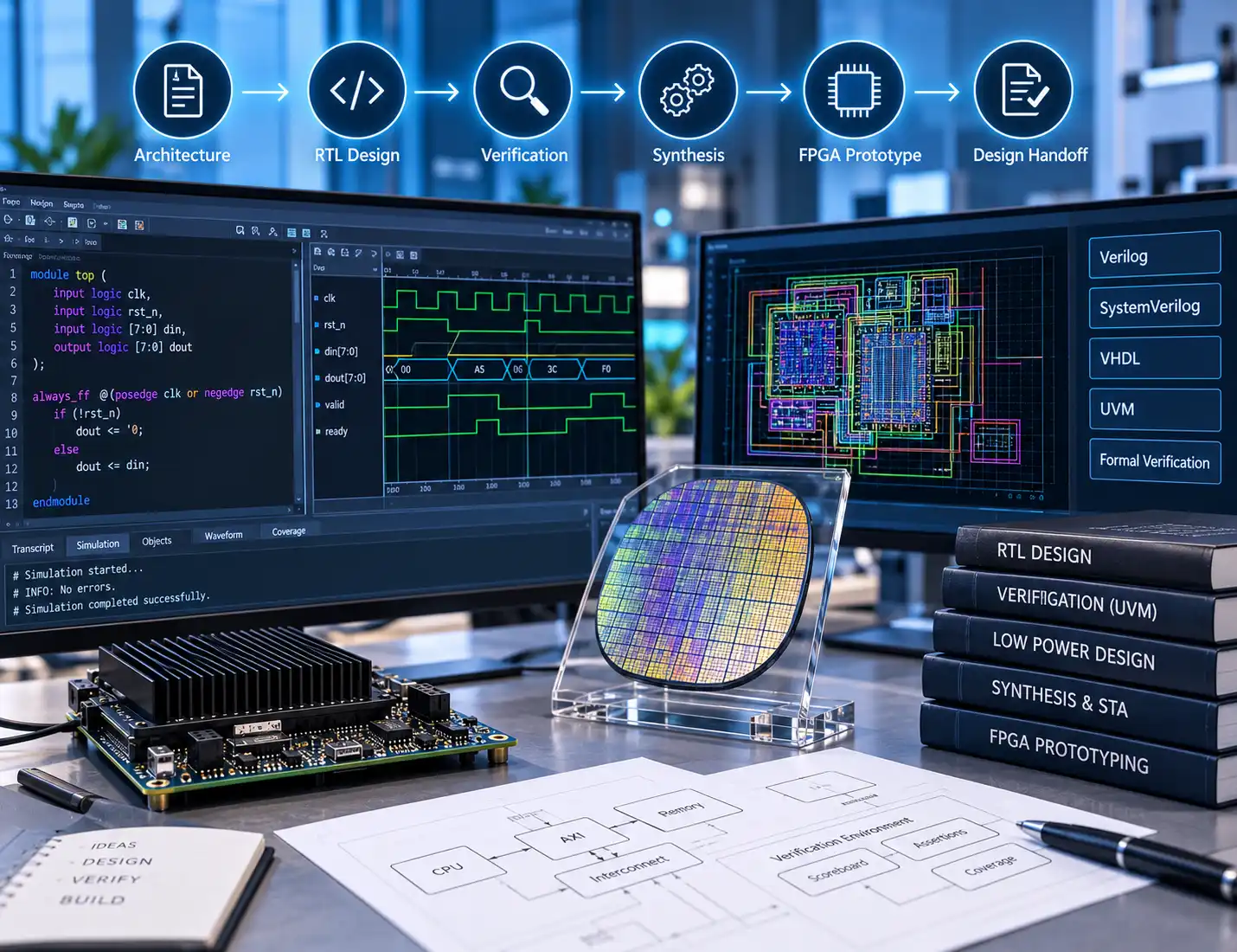
Relevant Adequate Infosoft Engineering Case Studies
Adequate Infosoft's public case studies primarily demonstrate downstream embedded product engineering rather than confidential semiconductor RTL. They remain relevant because VLSI decisions must ultimately support firmware, sensors, communication, power management, and real operating conditions.

ARM-Powered Wrist-Mounted Smart Device
This project incorporates ARM processor technology, personalized Android AOSP operating system, high-speed 5G connectivity, LiDAR gesture technology, and floating display. It serves as a showcase of system-level integration experience which is useful in specification of CPU, accelerators, memory, and I/O requirements.
Read Case Study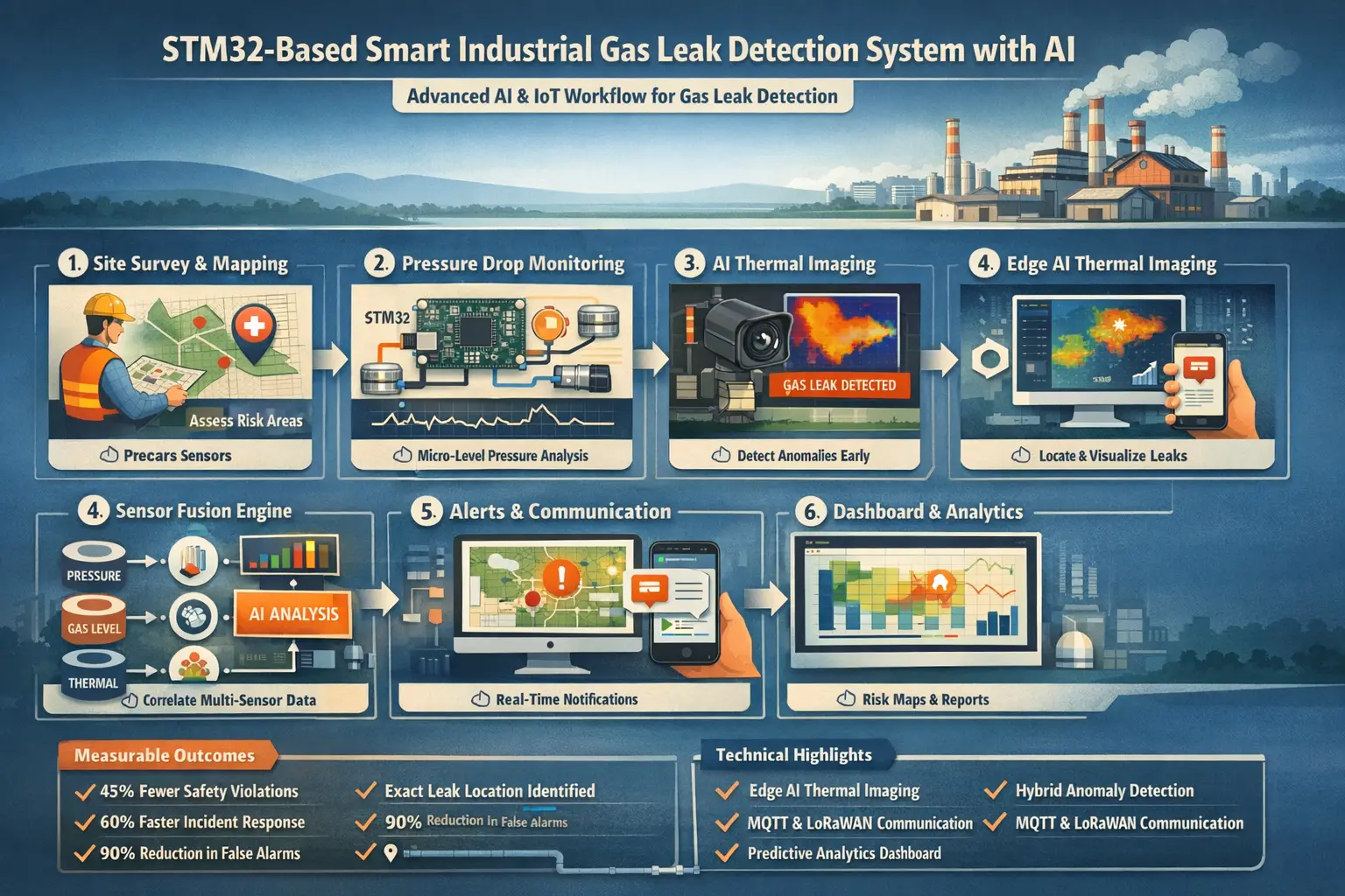
STM32-Based Industrial Gas Detection
The gas-detector system displays features like embedded sensing, real-time data processing, and alert systems. These features can be associated with the operations related to business regulation, the functions of data collection, interruptions, and communication.
Read Case Study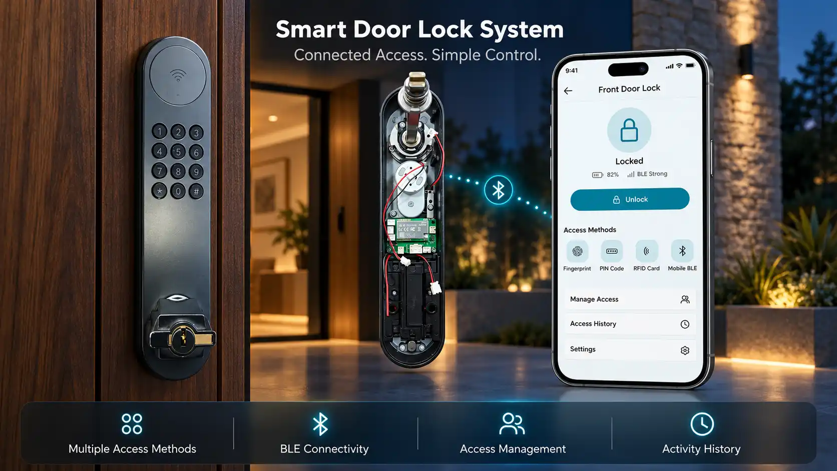
Nordic nRF52840 BLE Smart Lock
This connected access-control product combines secure embedded processing, BLE, fingerprint, RFID, PIN access, mobile applications, and cloud management. It illustrates how hardware architecture, firmware behavior, security, and communication reliability interact in a production-oriented IoT system.
Read Case StudyEnd-to-End Digital VLSI Engineering Services
Depending on the size of the project, we can either give you our specialized engineering engineering support or a whole team of digital design and verification experts.
We can begin any engagement from scratch, or we can help build on existing RTL codebase, work on an almost done verification environment or assist in getting scalabilities of an FPGA prototype into resemblance for ASIC system.
RTL Design and Microarchitecture Development
Our RTL design services convert algorithmic or product specifications into an exact and synthesizable hardware design. The designers develop data streams, control mechanisms, pipelines, the finite state machine, the registers interface, the arbitration algorithm, buffering, interruptions, and error recovery procedures before completing actual production of the RTL.
We develop reusable digital blocks such as:
Communication and protocol controllers DMA engines and data movers FIFOs, arbiters, bridges, and interconnect logic Memory controllers and register banks Sensor and peripheral interfaces Digital signal-processing pipelines Hardware accelerators Security and cryptographic control blocks Power, clock, reset, and interrupt controllers RISC-V peripherals and custom instruction support Packet-processing and industrial-control logic
The RTL is structured for readability, parameterization, predictable synthesis, and verification reuse. We apply explicit clock and reset strategies, avoid unintended latches, review signed and unsigned arithmetic, and consider overflow, underflow, backpressure, and illegal-state recovery.
For projects targeting both FPGA and ASIC implementation, technology-specific elements are isolated behind controlled interfaces. This helps the core logic remain portable while memories, clocking primitives, and physical I/O use platform-appropriate implementations.
ASIC and SoC Design Support
Adequate Infosoft supports digital ASIC and SoC development at block, subsystem, and integration levels. We help teams define IP boundaries, memory maps, address decoding, bus connectivity, interrupt routing, clock structures, reset sequencing, and hardware–software interfaces.
In systems on chip (SoC) based on Arm architecture, one can include logic around interfaces like AXI, AHB, and APB. According to Arm, AMBA consists of several protocols for communication on an integrated circuit.
AXI is designed for high-speed connections, while APB is used for low-bandwidth connections to external devices. In case of AXI and APB, designs are checked in terms of handshakes, bursts processing, order, possible responses, and backpressure.
In addition, RISC-V-based architectures are also supported to include processor incorporation, peripherals design, memory units registration, and so on. According to some architectural specifications, compliance tests are conducted to check compliance of designs.
Digital Verification and UVM Services
Verification should begin while the architecture is being defined, not after RTL completion. Our verification engineers convert the specification into a structured verification plan containing features, scenarios, assertions, coverage goals, negative tests, and completion criteria.
For complex IP and SoC environments, we develop SystemVerilog and UVM testbenches with:
Interface agents and reusable verification components Drivers, monitors, sequencers, and sequences Reference models and scoreboards Transaction-level models Register abstraction models Protocol and data-integrity checkers Constrained-random stimulus Directed corner-case tests Error injection and recovery scenarios Functional coverage models Automated regressions and result reporting
The Universal Verification Methodology has been standardized in accordance with IEEE 1800.2 and is continuously updated and maintained through the Accellera framework. Its component-based architecture allows engineers to develop flexible, scalable and reusable verification environments across various blocks or projects.
In addition, we can create an entirely new verification environment, enhance current testbenches, transfer verification IP content between one simulator and another, or study regressions that have become hard to reproduce or unstable over time.
Assertion-Based and Formal Verification
Simulation has its own merits, however, some important control properties, protocol properties, and safety properties are checked more effectively using assertions and formal methods. SystemVerilog Assertions are written for the interface rules, request-response timings, mutual exclusion, FIFO restrictions, legal changes in state, interrupt conditions, reset properties, and ordering of transactions.
The applications of formal verification include:
Control-centric RTL Access arbitration / control logic Deadlock and livelock analysis FIFO overflow / underflow prevention Protocol conformity Register and security policy behavior Checking of equivalence Analysis of unreachable states Initialization / reset property analysis
Properties are connected to specification requirements wherever possible. The results of formal analysis are scrutinized for assumptions, reachability verification, the depth of proof, and coverage based on which a passed property is accepted after considering the proof conditions.
Functional Coverage and Verification Closure
Running thousands of tests does not demonstrate that the important behavior has been exercised. Verification closure requires evidence that the implementation, testbench, assertions, and coverage model collectively address the intended design.
Our coverage process combines:
Statement, branch, expression, toggle, and FSM coverage Functional covergroups and cross coverage Assertion coverage Requirements traceability Regression stability Bug discovery and closure trends Reviewed coverage exclusions Targeted tests for uncovered scenarios
Coverage holes are classified before action. A gap may indicate missing stimulus, unreachable functionality, an incorrect model, disabled configuration, or incomplete RTL. Waivers are documented with technical justification rather than used simply to improve a percentage.
Design and Verification of Low-Power Digital Products
When it comes to semiconductor products that are sensitive to energy consumption, we should be thinking about the architecture stage of the design. We can help in finding clock gating, dead paths of data, memory access patterns, unnecessary switching and requirements for power domains.
Whenever a design is done in terms of IEEE 1801 Unified Power Format, our specialists will assist with defining or verifying power domains, isolation, retention, power switches and power states transition.
The low power verification can include the following:
Isolation before the turn off Restoration of the retained state Resetting after the power turn-off Outputs from inactive power domain are safe Conditions for enabling the clock gating Legality of power state sequence Counting communications in different power domains
The intent to design the product should comply with RTL, assumptions in the verification process, the behavior in the synthesis process and modes of operation to be used.
CDC, RDC, Lint, and RTL Quality Analysis
Clock-domain crossing and reset-domain crossing failures can evade mundane functionality simulation. We analyze synchronization structures, asynchronous controls, pulse transfer, multi-bit data transfer, reconvergence, fifo design, clock cross-referential, and reset releasing.
Our static quality procedure can include linting, CDC checking, RDC checking, elaboration checking, synthesis hints, and design guidelines verification. Problems are categorized according to real risks., so neglecting warnings could hide a silicon problem, but treating all warnings equally would over-engineer solutions.
We also provide help in modernizing inherited RTL, eliminating unsafe elements, enhancing parameterization, separating combinatorial and sequential logic, standardizing resets, and adding assertions and explanations about behavior.
FPGA Prototyping and Hardware Validation
FPGA prototyping provides an opportunity to validate digital logic with real peripherals, software, and data before an ASIC tape-out or product release. We port synthesizable RTL to suitable AMD/Xilinx, Intel, Lattice, Microchip, or comparable FPGA platforms.
Prototype development can include:
Clock and reset integration FPGA memory and interface adaptation Timing constraints On-chip logic analyzer integration Test firmware and register-access tools Hardware–software co-validation High-speed data-path evaluation Long-duration and stress testing
An FPGA prototype does not reproduce every ASIC characteristic, but it can expose architectural, integration, throughput, software, and real-time interaction problems earlier in the program.
Deliverables for Verification Automation and Engineering
In VLSI development, repeatability is key. This is achieved by creating scripts and continuous-integration processes for various tasks such as compilation, selection of tests, regression testing, management of seeds, log processing, coverage merging, and report generation.
Depending on the clients' needs, the scope of deliverables may encompass:
High-level and microarchitectural specs RTL source code and relevant configuration files UVM or module-level testbenches Verification plan and requirements matrix Assertions and properties Regression scripts and testing schedule Coverage reports and waiver documents Lint, CDC, RDC, and synthesis reports FPGAs prototype files Integration instructions and register documentation Error reports and verification closure documentation
The source code is under version control and the process of passing documentation from one party to another is clearly defined.
Frequently Asked Questions
We have ease with Verilog, SystemVerilog, VHDL, SystemVerilog Assertion, UVM along with scripting, directed verification, constrained random verification, formal verification and FPGA-based validation, etc.
Yes. We can review the specification and RTL, create an independent verification plan, develop or improve the testbench, run regressions, analyze coverage, and document defects and gaps.
Yes. We support reusable IP, ASIC-oriented RTL, FPGA implementation, FPGA prototyping, and design approaches that isolate technology-dependent components where portability is required.
Yes, we can check the structure of the test bench, stability of regression process, quality of coverage, the presence of bugs, dependencies of tools and gaps in verification plan before putting together the recovery plan.
Start Your Digital VLSI Project
Collaborate with Adequate Infosoft for organized RTL design, repeatable verification setups, coverage-based testing, and productive digital engineering. To initiate a technical evaluation, share your requirement, past design, verification strategy, or FPGA mock-up.
Editorial Resources