


 Mean Stack Development
 Vue JS Development
 Javascript Development
 React JS Development
 Angular JS Development
 Next JS development
 Java Development
 Python Development
 Django Development
 Cherrypy Development
 C# Development
 ASP.NET Development
 NodeJS Development
 Laravel Development
 CodeIgniter Development
 Zend Development
 Ruby on Rails Development
 CakePHP Development
 PHP Website Development
 Symfony Development
 Drupal Development
 Joomla Development
 Wordpress Development
 .NET Nuke Development
 Kentico
 Umbraco
 .NET MAUI Development
 Xamarin Application Development
 iOS Application Development
 Android Application Development
 Android Wear App Development
 Ionic Development
 iBeacon Application Development
 Universal Windows Platform (UWP)
 Kotlin Application Development
 Swift Application Development
 Flutter Application Development
 PWA Application Development
 Flutter Health Tech & Wearable App Development Company
 React Native Health Tech Wearable App Development
 Offshore Software Development
 Custom Application Development
 Front-End Development
 Full Stack Development
 AI & Machine Learning
 Custom CRM Solutions
 Flask Software Development
 Electron JS Development
 ChatGPT Development
 Telemedicine App Development
 Build Smart Telemedicine Platform
 Beauty & Salon App Solutions
 Hire Workato Experts
 Magento Development
 Magento 2.0 Development
 Magento Enterprise
 Shopping Cart Development
 Prestashop Development
 Shopify Development
 Open Cart Development
 WooCommerce Development
 BigCommerce Development
 NopCommerce Development
 Virto Commerce Development
 AspDotNetStorefront Development
 .NET Application Development
 Microsoft Dynamics CRM
 VB .NET Development
 Sharepoint Migration
 ASP.NET Core Development
 ASP.NET MVC Development
 AJAX Development
 Agile Development
 Microsoft Bot
 Microsoft Blazor
 Microsoft Azure Cognitive
 HTML 5
 UI/UX Design
 Graphic Design
 Adobe Photoshop
 XML Application Development
 Cloud Computing Solutions
 Azure Cloud App Development
 AWS Development
 Google Cloud Development
 Certified AWS IoT Services Developers
 DevOps Consulting & Development
 Kubernetes Consulting & Services
 SQL Programming Development
 MySQL Development
 MongoDB Development
 Big Data
 Robotic Process Automation
 Social Media Marketing
 Search Engine Optimization
 QA Testing
 Software Testing
 Software Security
 Maintenance And Support
 I.T. Consulting Services
 Business Intelligence
 YII Development
 Data Analysis
 Alexa Skills Development
 On Demand App for Mobile repairing services
 On Demand App for Car Service Booking
 On Demand App for Cleaning Services
 On Demand App for Pharmacy
 On Demand Dedicated Developers
 On Demand Lawyer App Development












 Nuki Smart Lock
 Salto Smart Lock
 TTlock Smart Lock
 NFC App Development
 Custom IOT Enabled Smart Lock
 Smart Locker Solutions
 Hospital Smart Lock Systems
 Hotel Smart Lock Systems
 Smart Home & Office Locks
 Smart Access for Schools & Colleges
 Unloc Smart Lock Integration
 Yale & August Smart Lock Integration
 Populife Smart Lock Integration
 Smart Lock Hardware Development
 Dairy IoT Solutions
 Agri IoT & AI Solutions
 Weather & Climate Solutions
 Water & Waste Management Solutions
 RaspBerry Pi
 Firmware Software Development
 ESP 32 Software Development
 Embedded Development
 Internet of Things
 Smart IoT Development
 IoT Sensor Integration & Development Solutions
 Smart IoT System Development for HVAC
 Tuya IoT App Development
 Particle IoT SDK
 IoT Development with AI
 Smart Pet GPS Tracker
 Dairy GPS Tracking Solutions
 GPS Fleet Management Software
 Car Rental & Subscription Solutions
 Car Buy & Sell Marketplace Development
 AI-Powered Car Wash App Development
 PCB Design & Fabrication
 IoT AC Automation
 AI–IoT Painting Solutions
 IoT Wearable Hardware & App Development
 HVAC Automation & AI Control Systems
 Smart Home IoT Engineering
 AI Embedded Systems
 AI Hardware Design Service
 Advanced IoT Hardware & Firmware Development
 Device Driver Development Services
 NXP i.MX RT Firmware & Hardware Services
 Microchip PIC & AVR Development
 Hire IoT Architects
 IoT Cloud & Infrastructure Solutions
 Infineon XMC / AURIX Development Services
 Matter & Thread IoT Services
 Native IoT Mobile App Development (BLE & Wi-Fi)
 Snapdragon IoT Firmware Development
 Renesas RA/RX Firmware Services
 Silicon Labs EFR32 Development Services
 Smart Wearable App Development
 Smart IoT Meters
 Smart Healthcare Wearable App Development
 Health Care Monitoring System
 Fitness Tracking App Development
 Smart Home Automation Apps
 nRF PCB Design
 ESP32 PCB Design
 Embedded Wearables Engineers
 Rental Property Management System
 Building Management System
 Smart Lighting Development
 Infineon Semiconductor Firmware Development Services
 Custom Camera Development: Hardware, Firmware & PCB Prototyping
 Smart Security Camera SDK
 Nordic Semiconductor SDK
 Infineon SDK
 Arduino SDK
 NFC Lock Integration
 Kerong Lock Integration
 IoT & AI Solutions for Manufacturing
 Smart Inventory & Logistics Solution
 Food & Beverage Industry Solutions
 Smart Hospitality Solutions
 Smart Property Management
 Custom Smart Home IOT SDK
 Smart IoT & AI in Healthcare
 AI-Powered Security Solutions
 Smart Home Safety & AI
 Veterinary Clinic Management (AI)
 Pet Care System (AI & IoT)
 Pet Training & Adoption (AI)
 Healthcare IoT Development
 Event Management Software
 Money Remittance App
 Money Lending App Development
 Utility and Bill Payment App
 IoT Mobile App Development (Flutter & React Native)
 AI & IoT Retail Solutions
 Smart EV App Development
 Smart Solar IoT & AI Solutions
 IoT-Based Energy Systems
 Smart Energy & Utilities Solutions
 6G Solutions
 IoT Security Solutions
 AI-Powered Lottery App Development
 AI-Sports Fitness Club Management
 Travel
 Real Estate
 Medical & Healthcare
 e-Learning
 Consumer Products
 Finance
 Automobile
 Media & Entertainment
 Billing Software
 Enterprise Resource Planning (ERP)
 Augumented & Virtual Reality
 Point of Sale(POS) Development
 Learning Management System
 EV Charging Solutions
 About Us
 Partners & Certifications
 Quality Assurance
 Our Clients & Testimonials
 Development Process
 Our Products
 Social Responsibility
 Work Ethics
 Vision & Mission
 Awards
 Live Project Demos
 Contact Us
 Case Studies
 Portfolio
 Blog
HDI & Fine-Pitch BGA PCB Design Services
Today's embedded devices are required to give higher processing power, connectivity and sensing function in smaller packages. The processors have hundreds of contacts placed on them and memory components should be placed close to the controller. Wearable gadgets and handheld computers require different approach to routing.
High-Density Interconnect, or HDI, PCB technology helps solve these challenges through smaller vias, finer traces, compact component placement and carefully planned multilayer structures.
Adequate Infosoft provides HDI PCB design and fine-pitch BGA layout services for industrial electronics, medical devices, cameras, wearables, robotics, automotive systems and connected IoT products.
Our engineers support hardware development from component selection and schematic review through layout, prototyping, board bring-up and manufacturing handover.
The goal is not simply to fit more components into a smaller area. A successful HDI design must remain electrically stable, thermally manageable, testable and practical to manufacture.
Let's Work Together!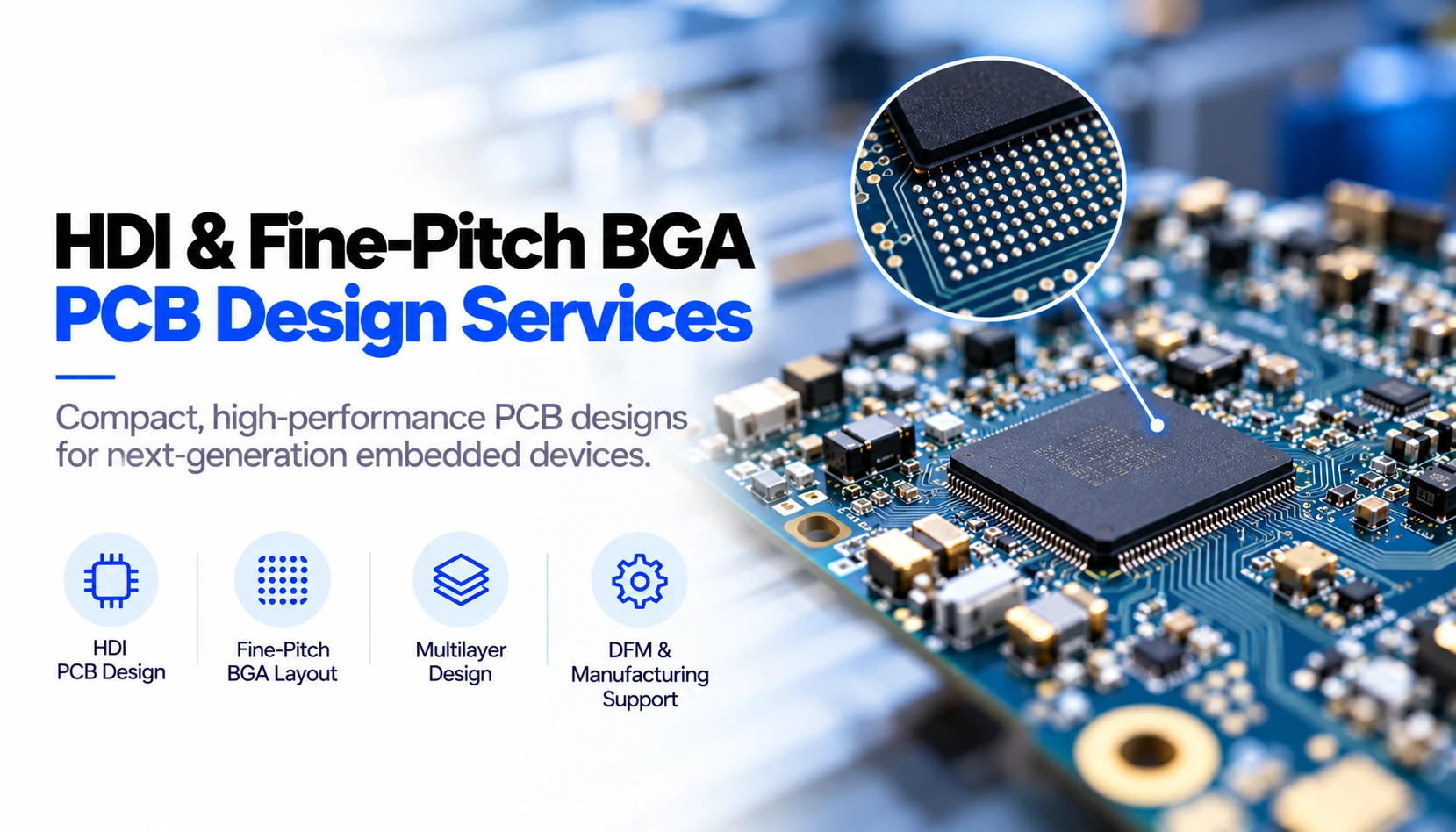
What Is an HDI PCB?
Compared to regular circuits' boards, HDI PCBs offer a greater density. Technologies like microvias and the via-in-pad process, as well as blind, buried, and stacked vias and fine-line technologies in routing, can be used in their design and construction.
These new methods make it possible for engineers to connect various microprocessors.
Fine-pitch BGA packages create a particular routing challenge because their connections are arranged beneath the component. The BGA pitch, pad size, number of rows, signal allocation and fabrication limits determine how the connections can escape into the wider PCB.
HDI technology is useful only when it is supported by a realistic fabrication and assembly plan. Adding microvias without considering reliability, cost and supplier capability can make production more difficult rather than easier.
Our HDI and Fine-Pitch BGA PCB Design Services
HDI Stack-Up Planning
We create the PCB stack-up based on routing density, impendence, power distribution, and manufacturer capabilities.
The design considers the number of signal layers, the use of reference planes, thicknesses of core and prepreg, weights of copper, kinds of dielectric materials used, and cycling of lamination. In case of a sequentially laminated board, the design of the via structure should be agreed with the manufacturer prior to the routing stage.
We support multilayer structures for compact embedded systems, including boards that combine digital processing, memory, sensors, RF and power-management circuits.
Fine-Pitch BGA Escape Routing
It is the layout of the assembly from which the BGA escape strategy commences. We evaluate ball pitch, pad sizes, via technology, signal sets, and number of routing layers allowed.
In accordance with the usage, the escape method may incorporate dog-bone fan-out, blind microvias, via-in-pad plated-over designs or a combination of these methods.
Power and ground balls are not treated as leftover connections. Their vias and plane connections form part of the power-delivery network and influence voltage stability, return paths and heat transfer.
Microvia and Via-in-Pad Engineering
The benefit of microvias is that they provide routing pathways underneath small-pitch components and significantly decrease the area used by typically drilled vias. Via-in-pad is especially useful for high-density BGAs and thermal pads but needs to have a proper manufacturing process.
In preparation for assembly, some processes may be needed to fill, coat and level the vias. If this process is done incorrectly, solder will flow through the open via and create an unreliable connection.
We prepare via requirements with the chosen PCB supplier and avoid unnecessary complexity where a lower-cost construction can satisfy the design.
Signal and Power Integrity
Compact routing enhances coupling capabilities of clock and memory, RF, and power circuitry.
During the design stage, we check impedance constraints, consistency of reference planes, differential pair routing, length restrictions, termination, decoupling, and return current paths. We also pay attention as to where to place regulators, crystals, oscillators, and sensitive analog components.
Power integrity is particularly important beneath high-pin-count devices. Decoupling components must be placed according to package and device requirements, with short connections to the appropriate power and ground structures.
Thermal Management
A dense layout can concentrate heat within a small area. We plan copper spreading, thermal vias, component spacing and enclosure contact where required.
Thermal strategy is developed around realistic operating modes instead of component maximum ratings alone. Processing workload, wireless transmission, charging and environmental temperature can all affect actual board conditions.
Featured Case Study: HDI STM32 Terminal for a Confidential IoT Client
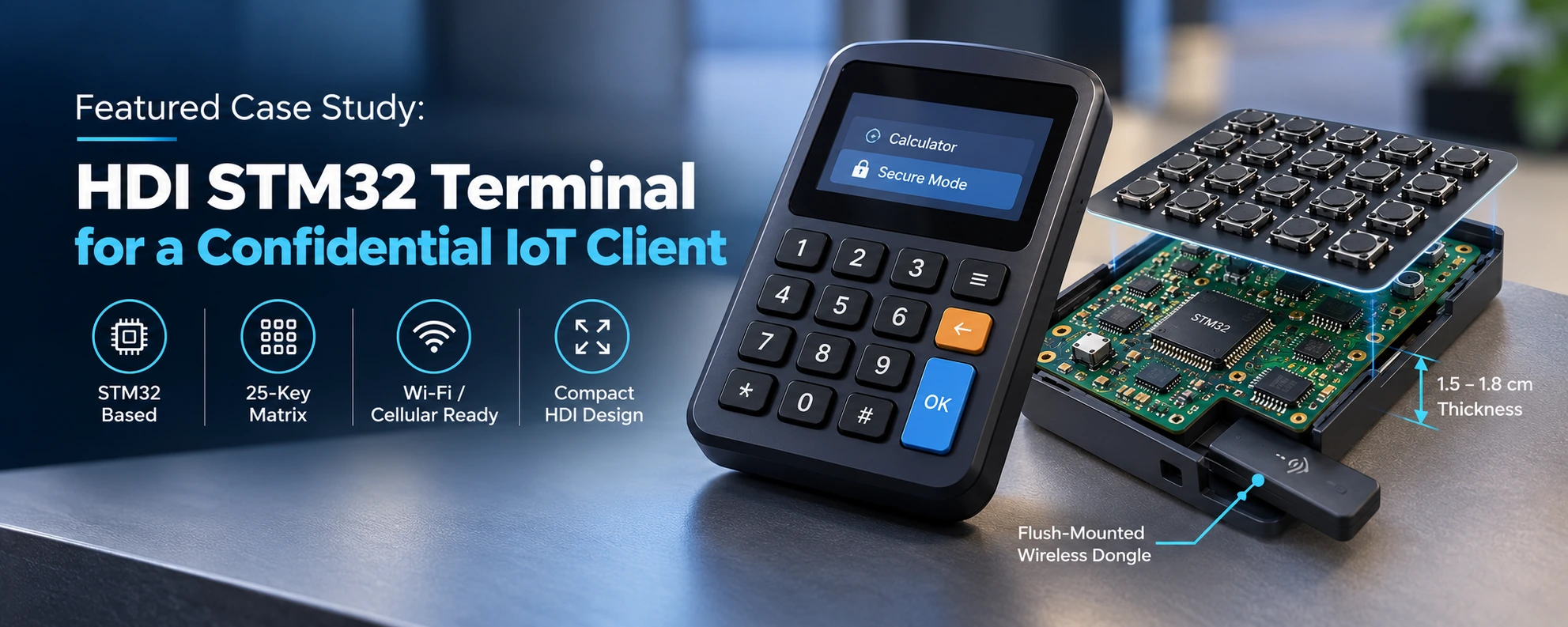
Client Requirement and Space Constraints
Adequate Infosoft was engaged by a client developing a specialized dual-mode IoT terminal. The client's company name is confidential, but the published project describes a compact device that could operate as a standard calculator and switch into a secured administrative terminal.
The final product design needed to stay in the thickness range of about 1.5 to 1.8 cm. The device must include a controller based on an STM32 chip implementing internal SMT, a button input matrix of 25 buttons, state indicators, safe firmware capability and a Wi-Fi or cellular connection.
If conventional printed circuit board design is applied, the product is likely to be thicker or to have an extra module outside the case. That is why the client wanted a high-density design based on co-design of mechanical and electrical components.
Four-Layer HDI Architecture
Our engineering team created a four-layer HDI PCB using a component-on-one-side strategy. The STM32 and supporting passive components were placed on the bottom, while the top surface was reserved for the 5 × 5 tactile-switch matrix.
With this arrangement, the switches could fit directly beneath the product overlay while ensuring that the processing electronics remained within the permitted internal height.
Microvia technology was employed to route the 25-key matrix without increasing the thickness of the printed circuit board. An internal ground plane acted as a reference thus ensuring that the controller and keypad signals are kept separate from switching noise generated by the external wireless link.
The layout also required careful treatment of the STM32 clock, power and programming connections. Decoupling paths were kept short, and access for firmware development and board bring-up was preserved despite the limited area.
Flush-Mounted Wireless Expansion
The external Wi-Fi or cellular dongle created both mechanical and electrical challenges. Mounting it conventionally would have exceeded the product's thickness target.
We incorporated a recessed USB/UART interface into the PCB cut-out allowing the dongle to rest inside the terminal profile. This design required collaboration on the board outline, connector alignment, enclosure design, and build process.
Cellular and wireless peripherals can create rapid load charge changes and generate signals at high frequency, thus requiring implementation of a special grounding and filtering system for the design.
Firmware, Prototype and Validation
The hardware employed a special STM32 bootloader operating in two modes. The normal mode operated as a regular calculator while the administrator mode, controlled by a PIN, was designed to activate the secure interface and enable the wireless connection. The T9-style input method allowed entering complicated configuration content through the 25-buttons keypad.
A functional proof of concept was built in a CNC-machined enclosure to verify fit and thermal performance. Pre-scan EMC testing was also performed to assess whether switching activity from the wireless dongle interfered with the terminal logic.
The project demonstrates our ability to combine HDI routing, microvias, mechanical integration, embedded firmware and compliance preparation in one compact product-development workflow.
Relevant Projects That Demonstrate Our High-Density PCB Experience
Our experience is supported by published projects involving compact multilayer boards, dense processing hardware and demanding component integration.
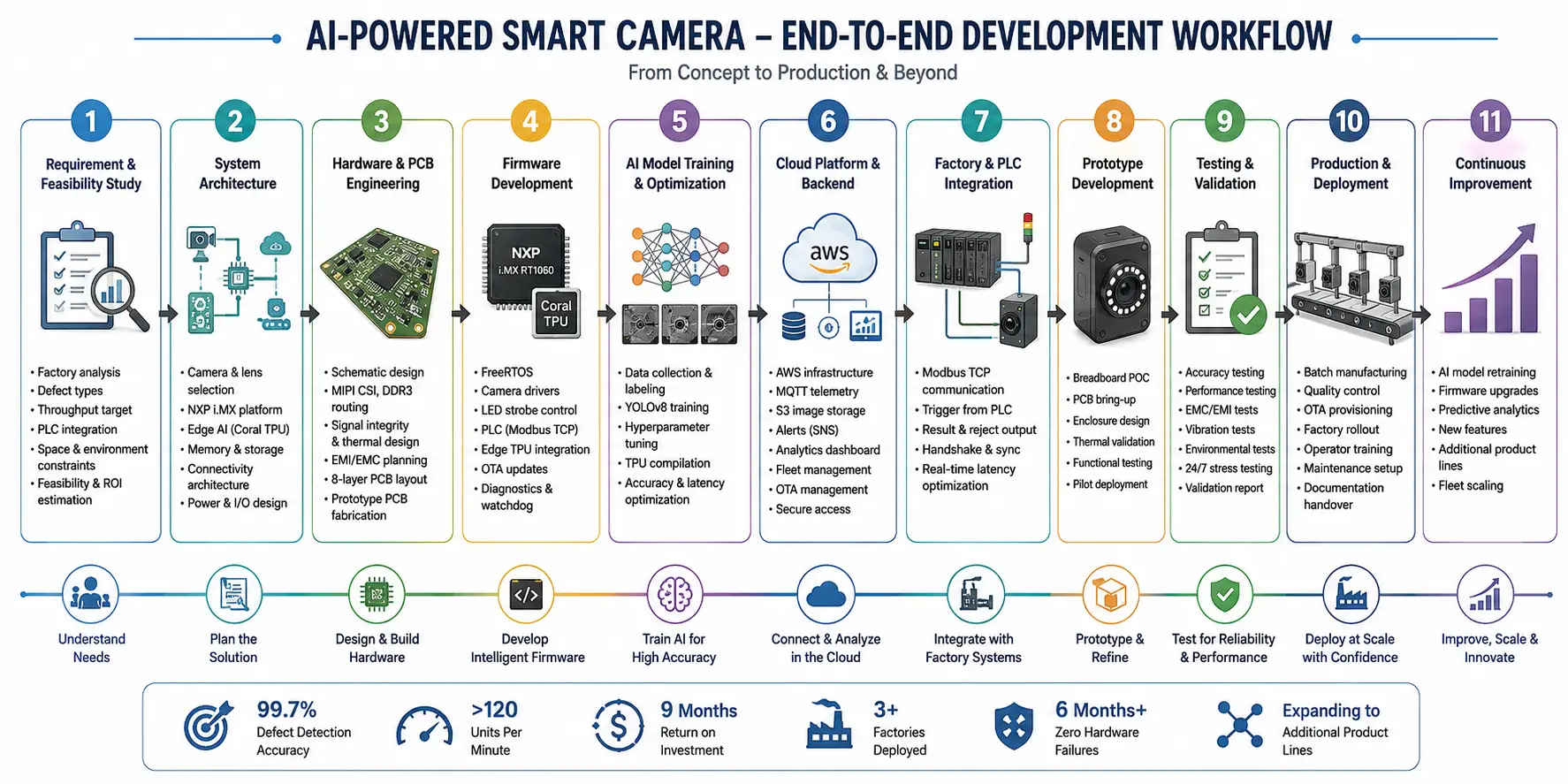
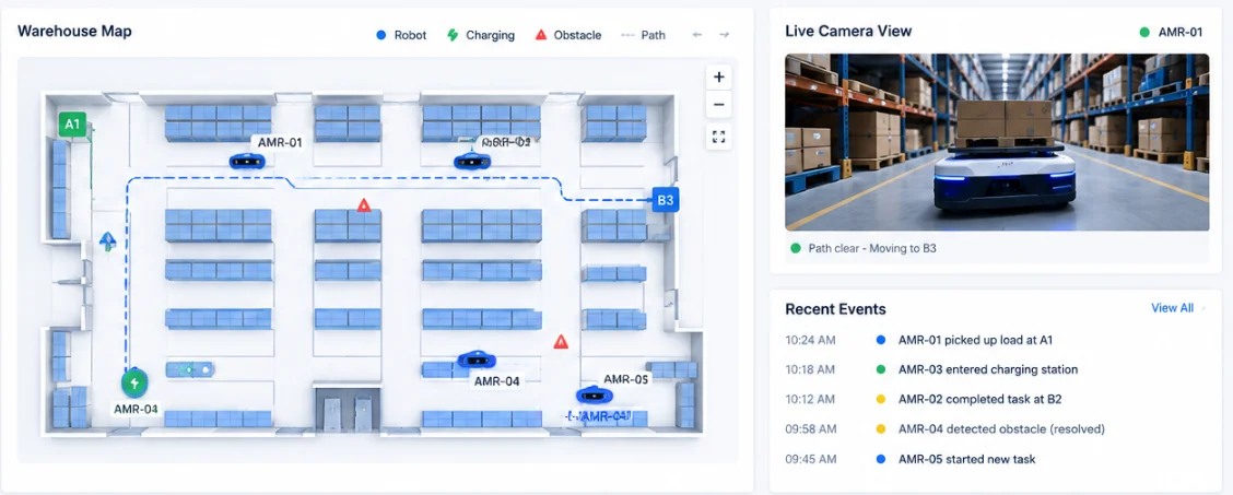
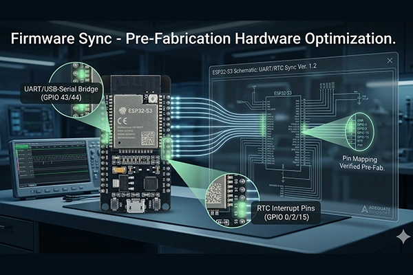
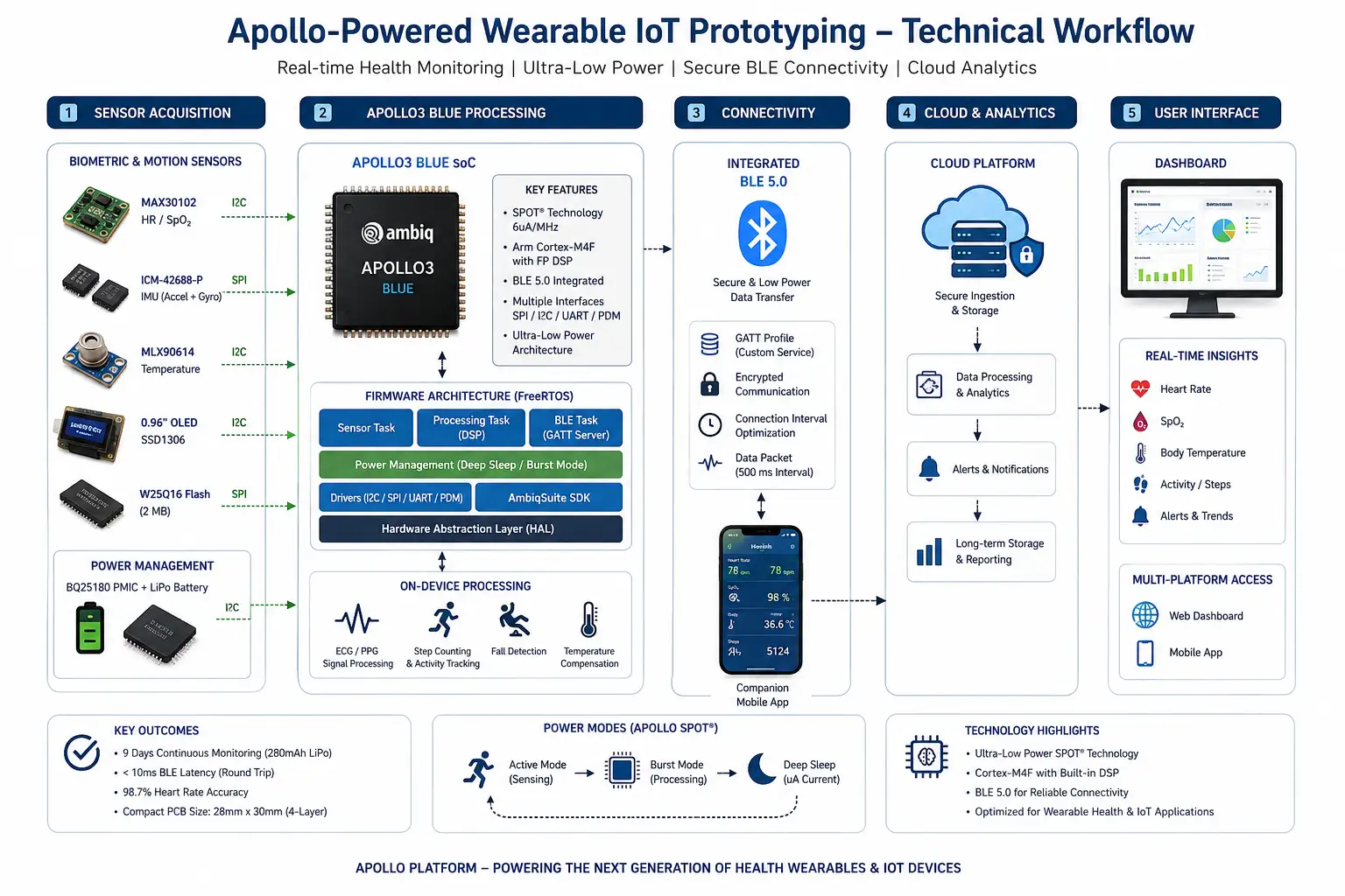
Design for Manufacturing and Assembly of HDI
The manufacturing process goes hand in hand with the design of HDI circuit boards. In order to begin generating fabrication outputs, the essential guidelines must be communicated to the board manufacturer.
The major production considerations are the following:
Size of the microvias and the laser drilling process utilized; The maximum permissible ratio in microvias; Sequential lamination; Methods of filling and capping the vias; The minimum widths or clearances of the traces; Copper positioning accuracy; Capability of fine-pitch solder masking; Surface finishing and flatness of the board; BGA stencils and solder paste applications; X-ray testing; Panelization and the necessary assembly tools.
Design for testing is also vital. When the majority of the area of the boards consists of small components, it can be difficult to place the test points. However, there should be an opportunity for gaining access to power, programming, reset, communication as well as manufacturing diagnostics.
Finalizing Manufacturing Deliverables
The deliverables at handover of our contract would include editable schematics, proprietary PCB source files, library of electronic components, stack-up drawings, impedance tables, files for manufacturing, drilling files, assembly files, BOMs, approved alternatives, files for placing the components.
In the case of complicated devices, we would additionally include programming guidance, bringing the circuit board to running, requirements for factory checking, and record of revisions.
The ownership of design files and their licenses from third parties are specified in the contract, thus the client is aware of the documents to be provided at the end of the contract.
Give Details About Your HDI PCB Project
In case your product features a small-pitch microprocessor, FPGA, memory component or small wearable construction, provide all the details about the package, the schematic diagram, the mechanical limitations and the manufacturing tasks to Adequate Infosoft.
The team of Adequate Infosoft can help in developing an HDI architecture that strikes a balance between board dimensions, electrical characteristics, manufacturing possibilities, assembly efficiency and production costs.
Frequently Asked Questions
The answer is no. The type of board needed ultimately depends on ball pitch, pin count, PCB dimensions, and layering design. Conventional fan-out may be suitable for larger packages, whereas the use of microvias and via-in-pad technology may be necessary for smaller packages.
There is no fixed number. Layer count depends on component density, BGA breakout, signal interfaces, power planes and EMC requirements. We select the simplest structure that meets the product’s technical needs.
Yes. We can review the schematic, package, stack-up, enclosure and manufacturer rules before developing a revised placement and escape-routing strategy.
Yes. We can coordinate prototype fabrication and assembly, including stencil planning, reflow requirements and X-ray inspection for hidden BGA joints where required.
Editorial Sources