


 Mean Stack Development
 Vue JS Development
 Javascript Development
 React JS Development
 Angular JS Development
 Next JS development
 Java Development
 Python Development
 Django Development
 Cherrypy Development
 C# Development
 ASP.NET Development
 NodeJS Development
 Laravel Development
 CodeIgniter Development
 Zend Development
 Ruby on Rails Development
 CakePHP Development
 PHP Website Development
 Symfony Development
 Drupal Development
 Joomla Development
 Wordpress Development
 .NET Nuke Development
 Kentico
 Umbraco
 .NET MAUI Development
 Xamarin Application Development
 iOS Application Development
 Android Application Development
 Android Wear App Development
 Ionic Development
 iBeacon Application Development
 Universal Windows Platform (UWP)
 Kotlin Application Development
 Swift Application Development
 Flutter Application Development
 PWA Application Development
 Flutter Health Tech & Wearable App Development Company
 React Native Health Tech Wearable App Development
 Offshore Software Development
 Custom Application Development
 Front-End Development
 Full Stack Development
 AI & Machine Learning
 Custom CRM Solutions
 Flask Software Development
 Electron JS Development
 ChatGPT Development
 Veterinary Telemedicine App Development
 Build Smart Telemedicine Platform
 Beauty & Salon App Solutions
 Hire Workato Experts
 Magento Development
 Magento 2.0 Development
 Magento Enterprise
 Shopping Cart Development
 Prestashop Development
 Shopify Development
 Open Cart Development
 WooCommerce Development
 BigCommerce Development
 NopCommerce Development
 Virto Commerce Development
 AspDotNetStorefront Development
 .NET Application Development
 Microsoft Dynamics CRM
 VB .NET Development
 Sharepoint Migration
 ASP.NET Core Development
 ASP.NET MVC Development
 AJAX Development
 Agile Development
 Microsoft Bot
 Microsoft Blazor
 Microsoft Azure Cognitive
 HTML 5
 UI/UX Design
 Graphic Design
 Adobe Photoshop
 XML Application Development
 Cloud Computing Solutions
 Azure Cloud App Development
 AWS Development
 Google Cloud Development
 Certified AWS IoT Services Developers
 DevOps Consulting & Development
 Kubernetes Consulting & Services
 SQL Programming Development
 MySQL Development
 MongoDB Development
 Big Data
 Robotic Process Automation
 Social Media Marketing
 Search Engine Optimization
 QA Testing
 Software Testing
 Software Security
 Maintenance And Support
 I.T. Consulting Services
 Business Intelligence
 YII Development
 Data Analysis
 Alexa Skills Development
 On Demand App for Mobile repairing services
 On Demand App for Car Service Booking
 On Demand App for Cleaning Services
 On Demand App for Pharmacy
 On Demand Dedicated Developers
 On Demand Lawyer App Development


 Nuki Smart Lock
 Salto Smart Lock
 TTlock Smart Lock
 NFC App Development
 Custom IOT Enabled Smart Lock
 Smart Locker Solutions
 Hospital Smart Lock Systems
 Hotel Smart Lock Systems
 Smart Home & Office Locks
 Smart Access for Schools & Colleges
 Unloc Smart Lock Integration
 Yale & August Smart Lock Integration
 Populife Smart Lock Integration
 Smart Lock Hardware Development
 Dairy IoT Solutions
 Agri IoT & AI Solutions
 Weather & Climate Solutions
 Water & Waste Management Solutions
 RaspBerry Pi
 Firmware Software Development
 ESP 32 Software Development
 Embedded Development
 Internet of Things
 Smart IoT Development
 IoT Sensor Integration & Development Solutions
 Smart IoT System Development for HVAC
 Tuya IoT App Development
 Particle IoT SDK
 IoT Development with AI
 Smart Pet GPS Tracker
 Dairy GPS Tracking Solutions
 GPS Fleet Management Software
 Car Rental & Subscription Solutions
 Car Buy & Sell Marketplace Development
 AI-Powered Car Wash App Development
 PCB Design & Fabrication
 IoT AC Automation
 AI–IoT Painting Solutions
 IoT Wearable Hardware & App Development
 HVAC Automation & AI Control Systems
 Smart Home IoT Engineering
 AI Embedded Systems
 AI Hardware Design Service
 Advanced IoT Hardware & Firmware Development
 Device Driver Development Services
 NXP i.MX RT Firmware & Hardware Services
 Microchip PIC & AVR Development
 Hire IoT Architects
 IoT Cloud & Infrastructure Solutions
 Infineon XMC / AURIX Development Services
 Matter & Thread IoT Services
 Native IoT Mobile App Development (BLE & Wi-Fi)
 Snapdragon IoT Firmware Development
 Renesas RA/RX Firmware Services
 Silicon Labs EFR32 Development Services
 Smart Wearable App Development
 Smart IoT Meters
 Smart Healthcare Wearable App Development
 Health Care Monitoring System
 Fitness Tracking App Development
 Smart Home Automation Apps
 nRF PCB Design
 ESP32 PCB Design
 Embedded Wearables Engineers
 Rental Property Management System
 Building Management System
 Smart Lighting Development
 Infineon Semiconductor Firmware Development Services
 Custom Camera Development: Hardware, Firmware & PCB Prototyping
 Smart Security Camera SDK
 Nordic Semiconductor SDK
 Infineon SDK
 Arduino SDK
 NFC Lock Integration
 Kerong Lock Integration
 IoT & AI Solutions for Manufacturing
 Smart Inventory & Logistics Solution
 Food & Beverage Industry Solutions
 Smart Hospitality Solutions
 Smart Property Management
 Custom Smart Home IOT SDK
 Smart IoT & AI in Healthcare
 AI-Powered Security Solutions
 Smart Home Safety & AI
 Veterinary Clinic Management (AI)
 Pet Care System (AI & IoT)
 Pet Training & Adoption (AI)
 Healthcare IoT Development
 Event Management Software
 Money Remittance App
 Money Lending App Development
 Utility and Bill Payment App
 IoT Mobile App Development (Flutter & React Native)
 AI & IoT Retail Solutions
 Smart EV App Development
 Smart Solar IoT & AI Solutions
 IoT-Based Energy Systems
 Smart Energy & Utilities Solutions
 6G Solutions
 IoT Security Solutions
 AI-Powered Lottery App Development
 AI-Sports Fitness Club Management
 Travel
 Real Estate
 Medical & Healthcare
 e-Learning
 Consumer Products
 Finance
 Automobile
 Media & Entertainment
 Billing Software
 Enterprise Resource Planning (ERP)
 Augumented & Virtual Reality
 Point of Sale(POS) Development
 Learning Management System
 EV Charging Solutions
 About Us
 Partners & Certifications
 Quality Assurance
 Our Clients & Testimonials
 Development Process
 Our Products
 Social Responsibility
 Work Ethics
 Vision & Mission
 Awards
 Live Project Demos
 Contact Us
 Case Studies
 Portfolio
 Blog
Low-Noise Biosignal PCB Design Services for Medical Devices
ECG, EEG, EMG and PPG devices measure signals that can be extremely small, easily disturbed and clinically important. A board that works well for a typical IoT sensor may fail to capture meaningful biosignals if switching noise, RF energy, ground currents, power ripple or poor electrode routing reaches the analog front end.
Adequate Infosoft provides low-noise biosignal PCB design services for medical devices, wellness wearables, sports technology and research instruments.
We create hardware for ECG, EEG, EMG, PPG, and other sensitive analog measurements with an emphasis on noise management, signal quality, power-saving techniques, firmware integration, and manufacturability.
Our involvement is not limited to the design of circuitry or PCB layout. We assist product developers in making engineering decisions that allow them to evaluate whether the received signal is clean enough for useful algorithm development, reproducibility of tests, and a successful roadmap.
Let's Work Together!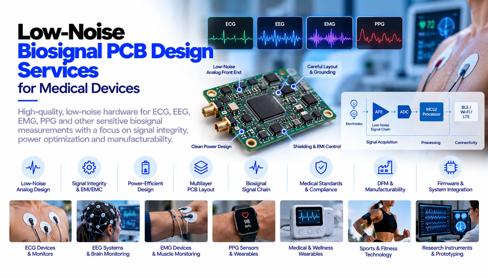
Sensitive Biosignal Measurement PCB Design
Biosignal devices are meant to detect electrical or optical data generated by the human body. For example, the ECG monitors cardiac electrical activities; EEG, low amplitude brain activities; EMG, muscles; while PPG uses light to calculate physiological parameters including pulse timing and blood volume.
These biosignals may get contaminated. Typical sources of this contamination are:
Ripple and edges of DC/DC converters Radio activity from Bluetooth, Wi-Fi and cellular radios Harmonics of digital clocking Badly isolated analog and digital return currents Large leakage currents and contamination at high-impedance inputs Long electrode traces and bad connector placement Motion artefacts and loose electrodes Noise generated by LED drivers in optical PPG devices Ground loops due to charging and USB connections
A good low noise design needs to consider the whole chain: sensors, protection, analog front-end, filtering, analogue-to-digital conversion, power delivery, layout, firmware timing and enclosures constraints.
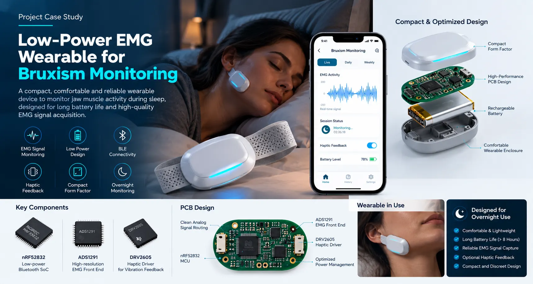
Project Case Study: Low-Power EMG Wearable for Bruxism Monitoring
Client and Product Goals
The medical wearable client needed an overnight portable device that would detect muscle movement in the jaws related to bruxism.
The device had to be able to collect low-frequency EMG signals at night, offer feedback based on vibrations if configured, and store or transmit data while being sufficiently comfortable to wear over time.
Among the most important requirements of the client was to ensure good quality of signals, low power consumption, small size of the board, and long working time exceeding eight hours.
The design could not treat the EMG front end as an independent circuit, since the product had a microcontroller, BLE interface, battery, and haptic motor on board.
Hardware and PCB Design Approach
Adequate Infosoft engineered the design around an nRF52832 microcontroller, an ADS1291 EMG acquisition analog front end and a DRV2605 haptic driver. The ADS1291 is designed for low-power, high-resolution biopotential acquisition, making it appropriate for the device's EMG capture requirements.
The PCB layout separated the sensitive analogue acquisition zone from BLE radio activity, digital clocks and haptic-drive transients. Input paths were kept short and carefully routed to reduce noise pickup. We used a star-grounding approach around the analogue section to help isolate the high-gain EMG signal chain from noisy digital and RF return currents.
Power planning was equally important. The analogue front end required stable, clean supply conditions, while the Bluetooth radio and vibration driver produced changing current demands. Local decoupling, thoughtful component placement and controlled power routing helped reduce the chance that these loads would affect the measured signal.
Firmware Integration and Outcome
The firmware controlled the synchronization of the EMG data capture process with the wearable operation modes, BLE connectivity, and haptic response behavior. This design considered the ability of the system to perform continuous overnight monitoring and efficient energy consumption.
In summary, the final approach presented to the client a compact wearable biosignal solution with better options for the future prototype validation and product development. The design also showed one important lesson in medical and wellness electronics, clean data starts with hardware decisions before anything else.
Relevant Adequate Infosoft Experience
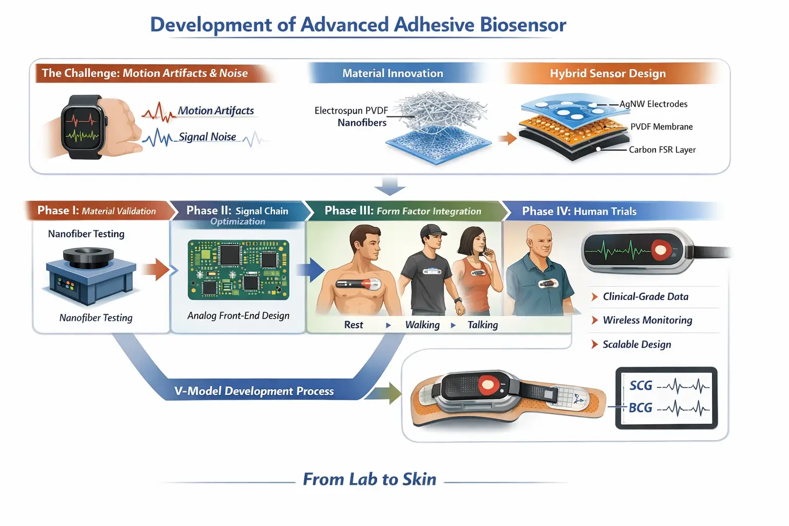
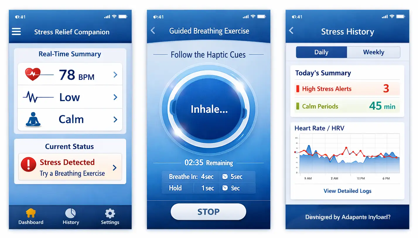
Our published work demonstrates experience across low-power embedded systems, wearable electronics, biosensors, BLE connectivity and health-focused digital products.

Our Low-Noise Medical PCB Design Capabilities
ECG, EEG and EMG Analog Front-End Design
The PCB layout is based on the use of dedicated analog front ends, instrumentation amplifiers, programmable gain amplifiers, reference sources and high resolution ADCs. The selection of components will depend on the number of channels, the input range, noise requirements, sampling speed, electrode array, battery size and the product application.
For biopotential signals, our design methodology may also incorporate input protection, RF interference (RFI) filter, lead-off detection facility, driven-reference or right leg drive arrangement, anti-aliasing filter and controlled gain stages.
A 24-bit biosignal AFE may provide good conversion performance, but PCB board noise can still affect actual performance. We concentrate on protecting the small analogue signal before it enters the converter instead of trying to "clean up" a bad acquisition using software alone.
PPG and Optical Biosensor PCB Design
PPG sensors consist of LEDs, photodiodes, analog signal capture and embedded processing all contained within an extremely compact package. The problem is that the optical signal can be much lower in level compared to the ambient light noise, LED switching, motion and power noise.
We design PPG sensors with LED-driver routing, photodiode circuit design, analogue and digital separation, low-noise power supplies, thermal design and mechanical design influencing optical coupling to the skin. We also time the hardware and firmware interaction to sample at appropriate points within the LED and ADC cycles.
This concept can prove beneficial for applications such as fitness tracking, sleep monitoring, wellness bands, remote patient monitoring and wearable research platforms.
Grounding, Layer Stack-Up and Return-Path Control
Grounding has always been one of the most misinterpreted aspects of biosignal PCB design. Splitting all the ground planes without proper knowledge of the current paths might worsen the situation. On the other hand, running high currents near the analog inputs will only decrease measurement accuracy.
We prepare our stack-up, placement of components and return paths of key signals prior to routing. In accordance with the architecture, it may include controlled analog section, short high-impedance inputs, reference plane continuity, splitting of noisy power supplies and clear interconnections between analog and digital domains.
In case of EMG, ECG and EEG applications, we will ensure that analog inputs have short routing, matched in case of differential routing and routed far from the clocks, antennas, inductors of switchers and high currents. The presence of charging circuits, USB interfaces and radios should be taken into account as well.
Power Integrity and Low-Power Wearable Design
Medical or wellness gadgets running on batteries demand both pure energy as well as longevity of operation. Linear regulators might be used for clean analogue rails, while certain switching regulators can help enhance the efficiency of batteries to meet digital rail requirements. It all depends on many factors.
For example, our solutions can include both analogue and digital supply filtering, local decoupling, reference supply protection, battery supervision and charging. All this is coordinated with firmware people so that communication devices, displays, haptics and high-power LEDs will not disturb capture times.
Firmware and Data-Acquisition Integration
PCB and firmware need to be designed as a single unit. We are able to provide SPI, I2C and interrupt-based communication among AFE, microcontroller and sensors. The design of firmware can incorporate sample time-stamping, variable gain, buffering, quality markers, lead-off, baseline, and secure transfer over BLE, Wi-Fi, or wired connectivity.
We are also able to support companion apps and cloud APIs for displaying the data from the devices, user management and capturing test data.
Our Engineering Process for Biosignal PCBs
The first thing we will need to think about is the measurement requirement: heart-rate sensing, muscle movement feedback, sleep analysis, stress evaluation, wellbeing data or research measurements. This will decide on electrode type, bandwidth, resolution, channel count, filtering, housing and testing approach.
Next, we look at the block diagram and select our analog front-end, microcontroller, radio and power management blocks.
Before we get into board-level routing, we decide on what goes where, important signal routes, stack-up and radio frequency location. We do not want to make changes in the future because of the addition of an antenna or switching converter.
In the course of design review, we verify that the schematic is clear, that creepage and clearance are defined where appropriate, decoupling scheme, protection circuitry, net class definitions, DFM/DFT requirements, and test-point accessibility have been considered.
We provide production-ready results such as schematic drawings, layouts, ODB++ or Gerber file generation, BOM calculations, picking and placement data, and assembly documentation.
Compliance with medical product regulations requires testing, risk management, and verification specific to each product. We take these requirements into account during our design process, but certification is only possible after passing all necessary regulatory processes.
Why Choose Adequate Infosoft for Biosignal PCB Design?
Structured and controlled engineering by cross-functional teams is crucial for low-noise biosignals. In our team, we have specialists competent in analogue circuit board design, firmware development, Bluetooth Low Energy technology, cloud connectivity and mobile apps development for solving issues concerning separation of the decisions made by hardware and software teams.
We use measurable specifications, clarify design compromises and create appropriate documentation that will be used for prototyping, review and manufacturing purposes. We support you at all stages from feasibility prototyping to refinement of your wearable device.
Frequently Asked Questions
The circuits measure extremely small signals; usually using high impedance electrodes. They are more prone to power noise, RF interference, poor ground, leakages, and motion artifacts as compared to general digital sensor devices.
Yes. This is important since ECG measures electrical biopotential, while PPG involves optical measurements. We take care of the power, analogue, optical and digital circuit design in such a way that there is no interference between them.
Yes. We support wearable hardware, low-power firmware, BLE connectivity, mobile apps, cloud APIs and manufacturing-ready PCB deliverables.
Sure. You just need to send us schematics, layouts, stack-up, grounding, power structure and firmware timings and we will be able to detect noise sources and come up with improvement plan.
We can assist with the engineering tasks related to the creation of good device, while certification, testing and other things related to regulations require a specific approach for a particular product.
Schematics, PCB design, Gerber/ODB++ files for manufacturing, BOM, placement file, assembly documentation and firmware/test documentation are some examples of typical outputs.